Package Information
www.vishay.com
Vishay Siliconix
Revison: 13-Feb-17
1
Document Number: 71655
THIS DOCUMENT IS SUBJECT TO CHANGE WITHOUT NOTICE. THE PRODUCTS DESCRIBED HEREIN AND THIS DOCUMENT
ARE SUBJECT TO SPECIFIC DISCLAIMERS, SET FORTH AT www.vishay.com/doc?91000
PowerPAK
®
SO-8, (Single/Dual)
DIM.
MILLIMETERS INCHES
MIN. NOM. MAX. MIN. NOM. MAX.
A 0.97 1.04 1.12 0.038 0.041 0.044
A1 - 0.05 0 - 0.002
b 0.33 0.41 0.51 0.013 0.016 0.020
c 0.23 0.28 0.33 0.009 0.011 0.013
D 5.05 5.15 5.26 0.199 0.203 0.207
D1 4.80 4.90 5.00 0.189 0.193 0.197
D2 3.56 3.76 3.91 0.140 0.148 0.154
D3 1.32 1.50 1.68 0.052 0.059 0.066
D4 0.57 typ. 0.0225 typ.
D5 3.98 typ. 0.157 typ.
E 6.05 6.15 6.25 0.238 0.242 0.246
E1 5.79 5.89 5.99 0.228 0.232 0.236
E2 3.48 3.66 3.84 0.137 0.144 0.151
E3 3.68 3.78 3.91 0.145 0.149 0.154
E4 0.75 typ. 0.030 typ.
e 1.27 BSC 0.050 BSC
K 1.27 typ. 0.050 typ.
K1 0.56 - - 0.022 - -
H 0.51 0.61 0.71 0.020 0.024 0.028
L 0.51 0.61 0.71 0.020 0.024 0.028
L1 0.06 0.13 0.20 0.002 0.005 0.008
- 12° - 12°
W 0.15 0.25 0.36 0.006 0.010 0.014
M 0.125 typ. 0.005 typ.
ECN: S17-0173-Rev. L, 13-Feb-17
DWG: 5881
3.
Dimensions exclusive of mold flash and cutting burrs.
1.
Notes
2
Inch will govern.
Dimensions exclusive of mold gate burrs.
Backside View of Single Pad
Backside View of Dual Pad
Detail Z
D
D1
D2
c
θ
A
θ
E1
θ
D1
E2
D2
e
b
1
2
3
4
H
4
3
2
1
θ
1
2
3
4
b
L
D2
D3 (2x)
Z
A1
K1
K
D
E
W
L1
D5
E3
D4
E4
E4
K
L
H
E2
D4
D5
M
E3
2
2
VISHAY SILICONIX
Power MOSFETs
Application Note AN821
PowerPAK
®
SO-8 Mounting and Thermal Considerations
APPLICATION NOTE
Revision: 16-Mai-13
1
Document Number: 71622
For technical questions, contact: powermosfettechsupport@vishay.com
THIS DOCUMENT IS SUBJECT TO CHANGE WITHOUT NOTICE. THE PRODUCTS DESCRIBED HEREIN AND THIS DOCUMENT
ARE SUBJECT TO SPECIFIC DISCLAIMERS, SET FORTH AT www.vishay.com/doc?91000
www.vishay.com
by Wharton McDaniel
MOSFETs for switching applications are now available with
die on resistances around 1 m and with the capability to
handle 85 A. While these die capabilities represent a major
advance over what was available just a few years ago, it is
important for power MOSFET packaging technology to keep
pace. It should be obvious that degradation of a high
performance die by the package is undesirable. PowerPAK
is a new package technology that addresses these issues.
In this application note, PowerPAK’s construction is
described. Following this mounting information is presented
including land patterns and soldering profiles for maximum
reliability. Finally, thermal and electrical performance is
discussed.
THE PowerPAK PACKAGE
The PowerPAK package was developed around the SO-8
package (figure 1). The PowerPAK SO-8 utilizes the same
footprint and the same pin-outs as the standard SO-8. This
allows PowerPAK to be substituted directly for a standard
SO-8 package. Being a leadless package, PowerPAK SO-8
utilizes the entire SO-8 footprint, freeing space normally
occupied by the leads, and thus allowing it to hold a larger
die than a standard SO-8. In fact, this larger die is slightly
larger than a full sized DPAK die. The bottom of the die
attach pad is exposed for the purpose of providing a direct,
low resistance thermal path to the substrate the device is
mounted on. Finally, the package height is lower than the
standard SO-8, making it an excellent choice for
applications with space constraints.
Fig. 1 PowerPAK 1212 Devices
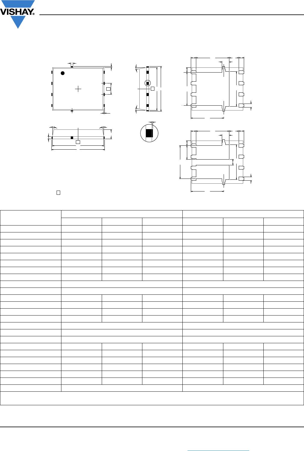
PowerPAK SO-8 SINGLE MOUNTING
The PowerPAK single is simple to use. The pin arrangement
(drain, source, gate pins) and the pin dimensions are the
same as standard SO-8 devices (see figure 2). Therefore, the
PowerPAK connection pads match directly to those of the
SO-8. The only difference is the extended drain connection
area. To take immediate advantage of the PowerPAK SO-8
single devices, they can be mounted to existing SO-8 land
patterns.
Fig. 2
The minimum land pattern recommended to take full
advantage of the PowerPAK thermal performance see
Application Note 826, Recommended Minimum Pad
Patterns With Outline Drawing Access for Vishay Siliconix
MOSFETs. Click on the PowerPAK SO-8 single in the index
of this document.
In this figure, the drain land pattern is given to make full
contact to the drain pad on the PowerPAK package.
This land pattern can be extended to the left, right, and top
of the drawn pattern. This extension will serve to increase
the heat dissipation by decreasing the thermal resistance
from the foot of the PowerPAK to the PC board and
therefore to the ambient. Note that increasing the drain land
area beyond a certain point will yield little decrease
in foot-to-board and foot-to-ambient thermal resistance.
Under specific conditions of board configuration, copper
weight and layer stack, experiments have found that
more than about 0.25 in
2
to 0.5 in
2
of additional copper
(in addition to the drain land) will yield little improvement in
thermal performance.
Standard SO-8 PowerPAK SO-8
PowerPAK
®
SO-8 Mounting and Thermal Considerations
APPLICATION NOTE
Application Note AN821
www.vishay.com
Vishay Siliconix
Revision: 16-Mai-13
2
Document Number: 71622
For technical questions, contact: powermosfettechsupport@vishay.com
THIS DOCUMENT IS SUBJECT TO CHANGE WITHOUT NOTICE. THE PRODUCTS DESCRIBED HEREIN AND THIS DOCUMENT
ARE SUBJECT TO SPECIFIC DISCLAIMERS, SET FORTH AT www.vishay.com/doc?91000
PowerPAK SO-8 DUAL
The pin arrangement (drain, source, gate pins) and the pin
dimensions of the PowerPAK SO-8 dual are the same as
standard SO-8 dual devices. Therefore, the PowerPAK
device connection pads match directly to those of the SO-8.
As in the single-channel package, the only exception is the
extended drain connection area. Manufacturers can likewise
take immediate advantage of the PowerPAK SO-8 dual
devices by mounting them to existing SO-8 dual land
patterns.
To take the advantage of the dual PowerPAK SO-8’s
thermal performance, the minimum recommended land
pattern can be found in Application Note 826,
Recommended Minimum Pad Patterns With Outline
Drawing Access for Vishay Siliconix MOSFETs. Click on the
PowerPAK 1212-8 dual in the index of this document.
The gap between the two drain pads is 24 mils. This
matches the spacing of the two drain pads on the
PowerPAK SO-8 dual package.
REFLOW SOLDERING
Vishay Siliconix surface-mount packages meet solder reflow
reliability requirements. Devices are subjected to solder
reflow as a test preconditioning and are then
reliability-tested using temperature cycle, bias humidity,
HAST, or pressure pot. The solder reflow temperature profile
used, and the temperatures and time duration, are shown in
figures 3 and 4.
For the lead (Pb)-free solder profile, see
www.vishay.com/doc?73257.
Fig. 3 Solder Reflow Temperature Profile
Fig. 4 Solder Reflow Temperatures and Time Durations
Ramp-Up Rate + 3 °C /s max.
Temperature at 150 - 200 °C 120 s max.
Temperature Above 217 °C 60 - 150 s
Maximum Temperature 255 + 5/- 0 °C
Time at Maximum
Temperature
30 s
Ramp-Down Rate + 6 °C/s max.
260 °C
3 °C(max) 6 ° C/s (max.)
30 s
217 °C
150 s (max.)
Reflow Zone
60 s (min.)
Pre-Heating Zone
150 - 200 °C
Maximum peak temperature at 240 °C is allowed.

SI7848BDP-T1-GE3

Mfr. #:
Manufacturer:
Vishay / Siliconix
Description:
MOSFET 40V Vds 20V Vgs PowerPAK SO-8
Lifecycle:
New from this manufacturer.
Delivery:
DHL FedEx Ups TNT EMS
Payment:
T/T Paypal Visa MoneyGram Western Union

Products related to this Datasheet