1
LTC1693
TYPICAL APPLICATION
U
DESCRIPTIO
U
FEATURES
APPLICATIO S
U
High Speed Single/Dual
N-Channel MOSFET Drivers
Dual MOSFET Drivers in SO-8 Package
or Single MOSFET Driver in MSOP Package
1G Electrical Isolation Between the Dual Drivers
Permits High/Low Side Gate Drive
1.5A Peak Output Current
16ns Rise/Fall Times at V
CC
= 12V, C
L
= 1nF
Wide V
CC
Range: 4.5V to 13.2V
CMOS Compatible Inputs with Hysteresis,
Input Thresholds are Independent of V
CC
Driver Input Can Be Driven Above V
CC
Undervoltage Lockout
Thermal Shutdown
The LTC
®
1693 family drives power N-channel MOSFETs
at high speed. The 1.5A peak output current reduces
switching losses in MOSFETs with high gate capacitance.
The LTC1693-1 contains two noninverting drivers while
the LTC1693-2 contains one noninverting and one invert-
ing driver. These dual drivers are electrically isolated and
independent. The LTC1693-3 is a single driver with an
output polarity select pin.
All MOSFET drivers offer V
CC
independent CMOS input
thresholds with 1.2V of typical hysteresis. They can level-
shift the input logic signal up or down to the rail-to-rail V
CC
drive for the external MOSFET.
The LTC1693 contains an undervoltage lockout circuit and
a thermal shutdown circuit that disable the external
N-channel MOSFET gate drive when activated.
The LTC1693-1 and LTC1693-2 come in an 8-lead SO pack-
age. The LTC1693-3 comes in an 8-lead MSOP package.
Power Supplies
High/Low Side Drivers
Motor/Relay Control
Line Drivers
Charge Pumps
Two Transistor Forward Converter
, LTC and LT are registered trademarks of Linear Technology Corporation.
12V
IN
BOOST
TG
TS
SENSE
+
SENSE
BG
PHASE
RUN/SHDN
V
FB
20
19
18
R6 100
R7 100
11
BAT54
12
16
14
13
R8
301k
1%
R2
5.1
R10
10k
1%
9
8
C15
0.1µF
C14
3300pF
C11
0.1µF
C12
100pF
C7
1µF
C8
1µF
C3
4700pF
25V
C4
0.1µF
L1
1.5µH
T1
13:2
V
OUT
1.5V/15A
RETURN
1693 TA01
C13
1µF
C1: SANYO 63MV330GX
C2: WIMA SMD4036/1.5/63/20/TR
C6: KEMET T510X477M006AS (×8)
L1: GOWANDA 50-318
T1: GOWANDA 50-319
C5
1µF
C10
0.1µF
C9
1800pF
5%
NPO
R9
12k
R5
2.49k
1%
15
17
2
1
12V
RETURN
V
IN
48VDC
±10%
4
3
5
6
7
10
SYNC
5V
REF
SL/ADJ
C
T
I
AVG
SS
V
C
V
REF
PGNDSGND
LT1339
LTC1693CS8-2
D2
MURS120
IN1
GND1
IN2
GND2
8
7
6
5
1
2
3
4
V
CC1
OUT1
V
CC2
OUT2
LTC1693CS8-2
IN1
GND1
IN2
GND2
8
7
6
5
1
2
3
4
V
CC1
OUT1
V
CC2
OUT2
D4
MBRO530T1
D3
MURS120
Q1
MTD20NO6HD
D1
MURS120
C2
1.5µF
63V
C1
330µF
63V
Q3
MTD20NO6HD
Q4
Si4420
R1
0.068
+
Q2
Si4420
×2
C6
470µF
6.3V
×8
+
R3
249
1%
R4
1.24k
1%
••
2
LTC1693
ABSOLUTE MAXIMUM RATINGS
W
WW
U
Supply Voltage (V
CC
) .............................................. 14V
Inputs (IN, PHASE) ...................................0.3V to 14V
Driver Output .................................0.3V to V
CC
+ 0.3V
GND1 to GND2 (Note 5) ..................................... ±100V
Junction Temperature.......................................... 150°C
Operating Ambient Temperature Range
C-Grade ................................................... 0°C to 70°C
I-Grade ................................................40°C to 85°C
Storage Temperature Range ................. 65°C to 150°C
Lead Temperature (Soldering, 10 sec)..................300°C
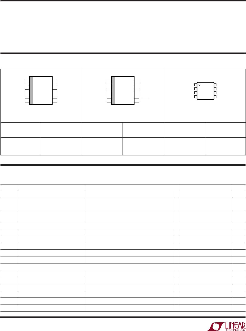
PACKAGE/ORDER INFORMATION
W
U
U
ORDER PART
NUMBER
S8 PART
MARKING
LTC1693-1CS8
LTC1693-1IS8
16931
16931I
1
2
3
4
8
7
6
5
TOP VIEW
V
CC1
OUT1
V
CC2
OUT2
IN1
GND1
IN2
GND2
S8 PACKAGE
8-LEAD PLASTIC SO
T
JMAX
= 150°C, θ
JA
= 135°C/W
1
2
3
4
8
7
6
5
TOP VIEW
V
CC1
OUT1
V
CC2
OUT2
IN1
GND1
IN2
GND2
S8 PACKAGE
8-LEAD PLASTIC SO
T
JMAX
= 150°C, θ
JA
= 135°C/W
ORDER PART
NUMBER
S8 PART
MARKING
LTC1693-2CS8
LTC1693-2IS8
16932
16932I
1
2
3
4
IN
NC
PHASE
GND
8
7
6
5
V
CC
OUT
NC
NC
TOP VIEW
MS8 PACKAGE
8-LEAD PLASTIC MSOP
T
JMAX
= 150°C, θ
JA
= 200°C/W
ORDER PART
NUMBER
MS8 PART
MARKING
LTC1693-3CMS8 LTEB
Consult factory for Industrial and Military grade parts.
ELECTRICAL CHARACTERISTICS
The denotes specifications which apply over the full operating
temperature range, otherwise specifications are at T
A
= 25°C. V
CC
= 12V, unless otherwise noted.
SYMBOL PARAMETER CONDITIONS MIN TYP MAX UNITS
V
CC
Supply Voltage Range 4.5 13.2 V
I
CC
Quiescent Current LTC1693-1, LTC1693-2, IN1 = IN2 = 0V (Note 2) 400 720 1100 µA
LTC1693-3, PHASE = 12V, IN = 0V
200 360 550 µA
I
CC(SW)
Switching Supply Current LTC1693-1, LTC1693-2, C
OUT
= 4.7nF, f
IN
= 100kHz 14.4 20 mA
LTC1693-3, C
OUT
= 4.7nF, f
IN
= 100kHz 7.2 10 mA
Input
V
IH
High Input Threshold 2.2 2.6 3.1 V
V
IL
Low Input Threshold 1.1 1.4 1.7 V
I
IN
Input Pin Bias Current ±0.01 ±10 µA
V
PH
PHASE Pin High Input Threshold (Note 3) 4.5 5.5 6.5 V
I
PH
PHASE Pin Pull-Up Current PHASE = 0V (Note 3) 10 20 45 µA
Output
V
OH
High Output Voltage I
OUT
= –10mA 11.92 11.97 V
V
OL
Low Output Voltage I
OUT
= 10mA 30 75 mV
R
ONL
Output Pull-Down Resistance 2.85
R
ONH
Output Pull-Up Resistance 3.00
I
PKL
Output Low Peak Current 1.70 A
I
PKH
Output High Peak Current 1.40 A
(Note 1)
3
LTC1693
ELECTRICAL CHARACTERISTICS
SYMBOL PARAMETER CONDITIONS MIN TYP MAX UNITS
Switching Timing (Note 4)
t
RISE
Output Rise Time C
OUT
= 1nF 17.5 35 ns
C
OUT
= 4.7nF 48.0 85 ns
t
FALL
Output Fall Time C
OUT
= 1nF 16.5 35 ns
C
OUT
= 4.7nF 42.0 75 ns
t
PLH
Output Low-High Propagation Delay C
OUT
= 1nF 38.0 70 ns
C
OUT
= 4.7nF 40.0 75 ns
t
PHL
Output High-Low Propagation Delay C
OUT
= 1nF 32 70 ns
C
OUT
= 4.7nF 35 75 ns
Driver Isolation
R
ISO
GND1-GND2 Isolation Resistance LTC1693-1, LTC1693-2 GND1-to-GND2 Voltage = 75V 0.075 1 G
Note 1: Absolute Maximum Ratings are those values beyond which the life
of a device may be impaired.
Note 2: Supply current is the total current for both drivers.
Note 3: Only the LTC1693-3 has a PHASE pin.
Note 4: All AC timing specificatons are guaranteed by design and are not
production tested.
Note 5: Only applies to the LTC1693-1 and LTC1693-2.
TYPICAL PERFOR A CE CHARACTERISTICS
UW
IN Threshold Voltage vs V
CC
TEMPERATURE (°C)
–50
INPUT THRESHOLD HYSTERESIS (V)
1.2
1.3
1.4
25 75
1693 G03
1.1
1.0
25 0 50 100 125
0.9
0.8
V
CC
= 12V
V
IH
-V
IL
IN Threshold Hysteresis
vs Temperature
IN Threshold Voltage
vs Temperature
V
CC
(V)
5
2.00
2.25
2.75
810
1693 G01
1.75
1.50
67
91112
1.25
1.00
2.50
INPUT THRESHOLD VOLTAGE (V)
V
IH
V
IL
T
A
= 25°C
TEMPERATURE (°C)
–50
INPUT THRESHOLD VOLTAGE (V)
2.75
25
1693 G02
2.00
1.50
–25 0 50
1.25
1.00
3.00
2.50
V
IH
V
IL
2.25
1.75
75 100 125
V
CC
= 12V
The denotes specifications which apply over the full operating
temperature range, otherwise specifications are at T
A
= 25°C. V
CC
= 12V, unless otherwise noted.

LTC1693-3CMS8#PBF

Mfr. #:
Manufacturer:
Analog Devices / Linear Technology
Description:
Gate Drivers High Speed MOSFET Driver
Lifecycle:
New from this manufacturer.
Delivery:
DHL FedEx Ups TNT EMS
Payment:
T/T Paypal Visa MoneyGram Western Union