8
LTC1693
APPLICATIONS INFORMATION
WUU
U
Overview
The LTC1693 single and dual drivers allow 3V- or 5V-based
digital circuits to drive power MOSFETs at high speeds. A
power MOSFET’s gate-charge loss increases with switch-
ing frequency and transition time. The LTC1693 is capable
of driving a 1nF load with a 16ns rise and fall time using a
V
CC
of 12V. This eliminates the need for higher voltage
supplies, such as 18V, to reduce the gate charge losses.
The LTC1693’s 360µA quiescent current is an order of
magnitude lower than most other drivers/buffers. This
improves system efficiency in both standby and switching
operation. Since a power MOSFET generally accounts for
the majority of power loss in a converter, addition of the
LT1693 to a high power converter design greatly improves
efficiency, using very little board space.
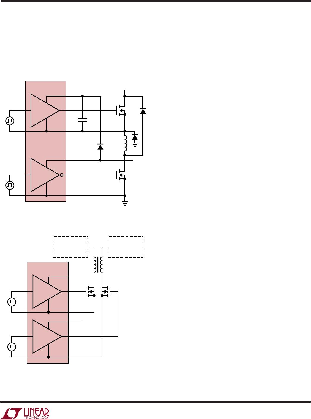
The LTC1693-1 and LTC1693-2 are dual drivers that are
electrically isolated. Each driver has independent opera-
tion from the other. Drivers may be used in different parts
of a system, such as a circuit requiring a floating driver and
the second driver being powered with respect to ground.
Input Stage
The LTC1693 employs 3V CMOS compatible input thresh-
olds that allow a low voltage digital signal to drive
standard
power MOSFETs. The LTC1693 incorporates a 4V internal
regulator to bias the input buffer. This allows the 3V CMOS
compatible input thresholds (V
IH
= 2.6V, V
IL
= 1.4V) to be
independent of variations in V
CC
. The 1.2V hysteresis
between V
IH
and V
IL
eliminates false triggering due to
ground noise during switching transitions. The LTC1693’s
input buffer has a high input impedance and draws less
than 10µA during standby.
Output Stage
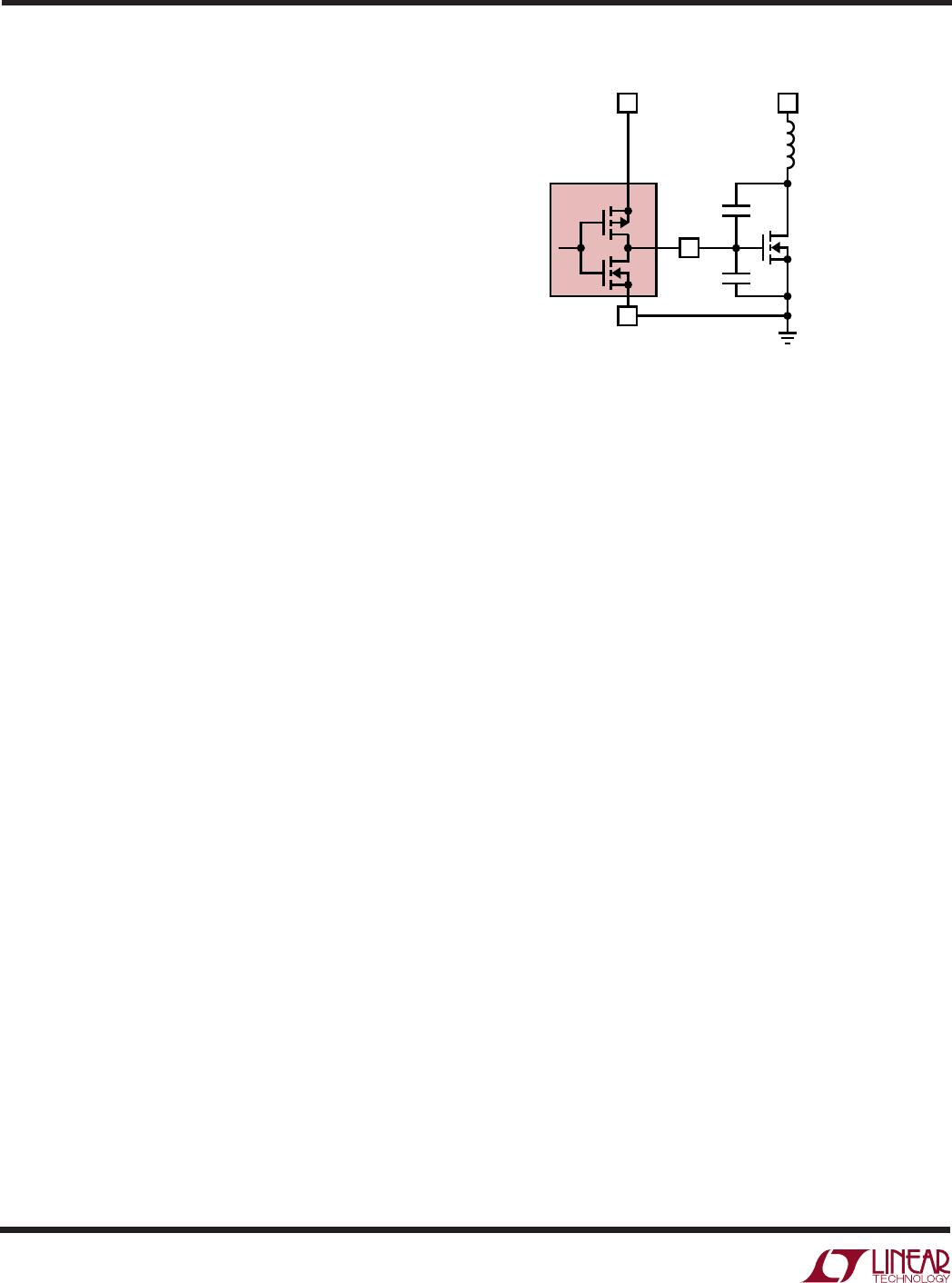
The LTC1693’s output stage is essentially a CMOS in-
verter, as shown by the P- and N-channel MOSFETs in
Figure 1 (P1 and N1). The CMOS inverter swings rail-to-
rail, giving maximum voltage drive to the load. This large
voltage swing is important in driving external power
MOSFETs, whose R
DS(ON)
is inversely proportional to its
gate overdrive voltage (V
GS
– V
T
).
P1
C
GD
V
DRAIN
POWER
MOSFET
L
EQ
(LOAD INDUCTOR
OR STRAY LEAD
INDUCTANCE)
C
GS
OUT
GND
LTC1693
1693 F01
N1
V
+
V
CC
Figure 1. Capacitance Seen by OUT During Switching
The LTC1693’s output peak currents are 1.4A (P1) and
1.7A (N1) respectively. The N-channel MOSFET (N1) has
higher current drive capability so it can discharge the
power MOSFET’s gate capacitance during high-to-low
signal transitions. When the power MOSFET’s gate is
pulled low by the LTC1693, its drain voltage is pulled high
by its load (e.g., a resistor or inductor). The slew rate of the
drain voltage causes current to flow back to the MOSFETs
gate through its gate-to-drain capacitance. If the MOSFET
driver does not have sufficient sink current capability (low
output impedance), the current through the power
MOSFET’s Miller capacitance (C
GD
) can momentarily pull
the gate high, turning the MOSFET back on.
Rise/Fall Time
Since the power MOSFET generally accounts for the ma-
jority of power lost in a converter, it’s important to quickly
turn it either fully “on” or “off” thereby minimizing the tran-
sition time in its linear region. The LTC1693 has rise and
fall times on the order of 16ns, delivering about 1.4A to 1.7A
of peak current to a 1nF load with a V
CC
of only 12V.
The LTC1693’s rise and fall times are determined by the
peak current capabilities of P1 and N1. The predriver,
shown in Figure 1 driving P1 and N1, uses an adaptive
method to minimize cross-conduction currents. This is
done with a 6ns nonoverlapping transition time. N1 is fully
turned off before P1 is turned-on and vice-versa using this
6ns buffer time. This minimizes any cross-conduction
currents while N1 and P1 are switching on and off yet is
short enough to not prolong their rise and fall times.