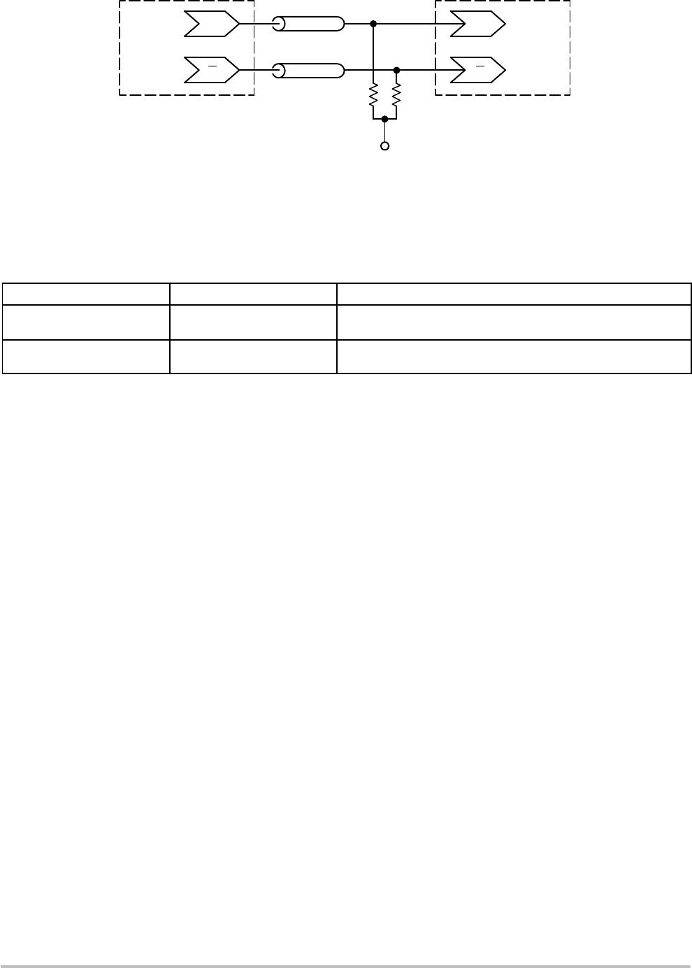
NB4N441
http://onsemi.com
10
Jitter Performance
Jitter is a common parameter associated with clock
generation and distribution. Clock jitter can be defined as the
deviation in a clock’s output transition from its
ideal position.
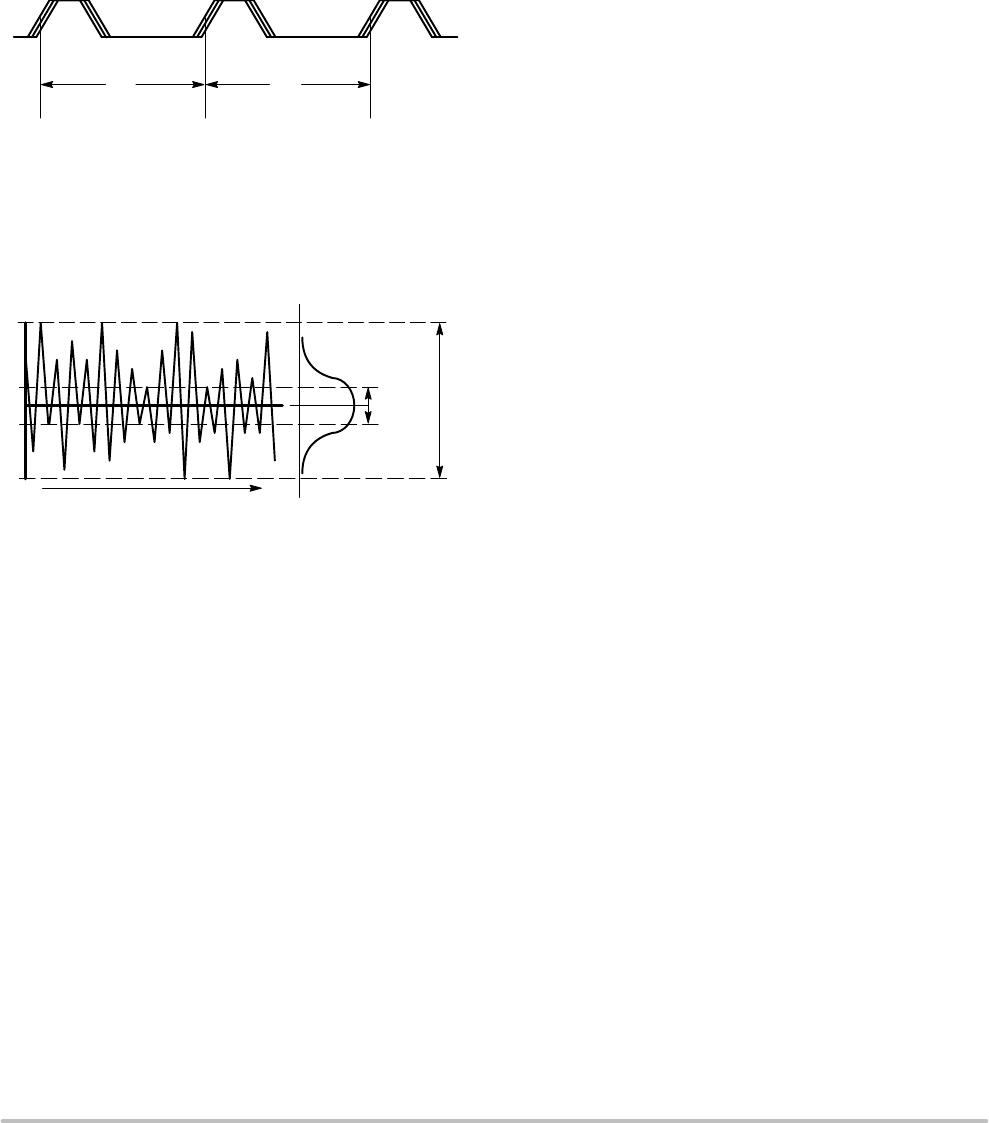
Cycle−to−Cycle Jitter (short−term) is the period
variation between two adjacent cycles over a defined
number of observed cycles. The number of cycles observed
is application dependent but the JEDEC specification is
1000 cycles.
Figure 8. Cycle−to−Cycle Jitter
T
JITTER(cycle−cycle)
= T
1
− T
0
T
0
T
1
Peak−to−Peak Jitter is the difference between the
highest and lowest acquired value and is represented as the
width of the Gaussian base.
Figure 9. Peak−to−Peak Jitter
Time
Typical
Gaussian
Distribution
RMS
or one
Sigma
Jitter
Jitter Amplitude
Peak−to−Peak Jitter (8 s)
There are different ways to measure jitter and often they
are confused with one another. The typical method of
measuring jitter is to look at the timing signal with an
oscilloscope and observe the variations in period−to−period
or cycle−to−cycle. If the scope is set up to trigger on every
rising or falling edge, set to infinite persistence mode and
allowed to trace sufficient cycles, it is possible to determine
the maximum and minimum periods of the timing signal.
Digital scopes can accumulate a large number of cycles,
create a histogram of the edge placements and record
peak−to−peak as well as standard deviations of the jitter.
Care must be taken that the measured edge is the edge
immediately following the trigger edge. These scopes can
also store a finite number of period durations and
post−processing software can analyze the data to find the
maximum and minimum periods.
Recent hardware and software developments have
resulted in advanced jitter measurement techniques. The
Tektronix TDS−series oscilloscopes have superb jitter
analysis capabilities on non−contiguous clocks with their
histogram and statistics capabilities. The Tektronix
TDSJIT2/3 Jitter Analysis software provides many key
timing parameter measurements and will extend that
capability by making jitter measurements on contiguous
clock and data cycles from single−shot acquisitions.
M1 by Amherst was used as well and both test methods
correlated.
Long−Term Period Jitter is the maximum jitter
observed at the end of a period’s edge when compared to the
position of the perfect reference clock’s edge and is specified
by the number of cycles over which the jitter is measured.
The number of cycles used to look for the maximum jitter
varies by application but the JEDEC spec is
10,000 observed cycles.
The NBC4N441 exhibit long term and cycle−to−cycle
jitter, which rivals that of SAW based oscillators. This jitter
performance comes with the added flexibility associated
with a synthesizer over a fixed frequency oscillator. The
jitter data presented should provide users with enough
information to determine the effect on their overall timing
budget. The jitter performance meets the needs of most
system designs while adding the flexibility of frequency
margining and field upgrades. These features are not
available with a fixed frequency SAW oscillator.