NB4N441
http://onsemi.com
6
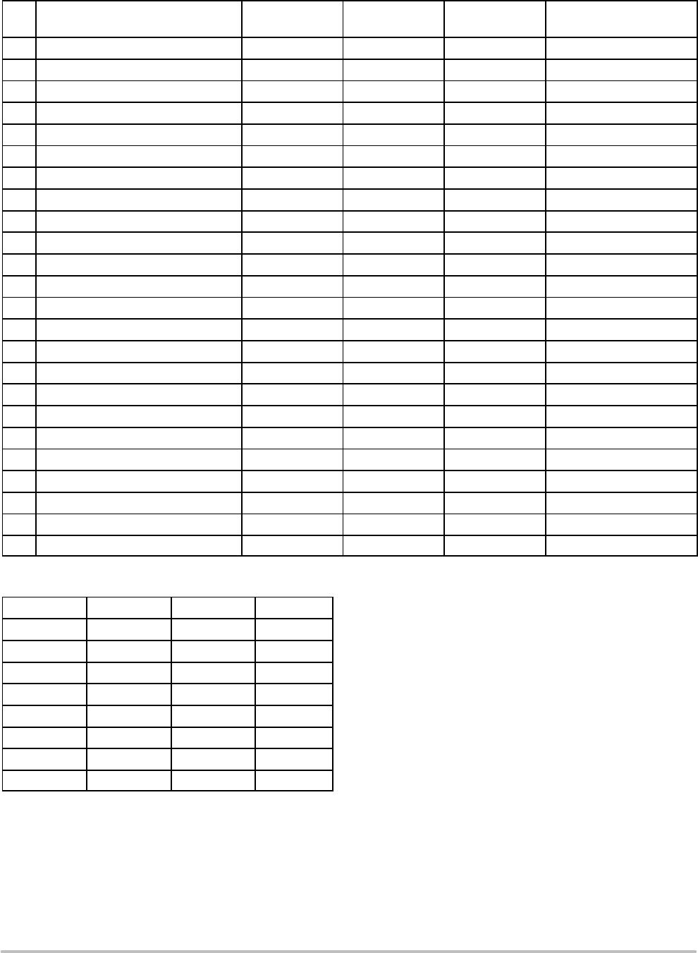
Table 6. DC CHARACTERISTICS V
CC
= 3.135 V to 3.465 V, GND = 0 V, T
A
= −40°C to +85°C
Symbol
Characteristic Min Typ Max Unit
I
CC
Power Supply Current (Inputs and Outputs Loaded) 50 70 90 mA
I
CCPLL
PLL Power Supply Current 10 20 30 mA
V
OH
LVPECL Output HIGH Voltage (Notes 4 and 5)
V
CC
= 3.3 V
V
CC
– 1145
2155
V
CC
− 1030
2270
V
CC
– 895
2405
mV
V
OL
LVPECL Output LOW Voltage (Notes 4 and 5)
V
CC
= 3.3 V
V
CC
– 1945
1355
V
CC
− 1760
1540
V
CC
– 1695
1605
mV
V
OHTTL
Output HIGH Voltage (LOCKED Pin) I
OH
= −0.8 mA 2.5 V
CC
V
V
OLTTL
Output LOW Voltage (LOCKED Pin) GND 0.4 V
V
IH
Input HIGH Voltage (LVTTL/LVCMOS) 2.0 V
CC
V
V
IL
Input LOW Voltage (LVTTL/LVCMOS) GND 0.8 V
I
IH
Input HIGH Current, OE V
IN
= 2.7 V, VCC
max
SCLK, SDATA, SLOAD V
IN
= 2.7 V, VCC
max
OE, SCLK, SDATA, SLOAD V
IN
= V
CC
, VCC
max
6.0
20
20
26
60
60
mA
mA
I
IL
Input LOW Current V
IN
= 0.5 V, VCC
max
10
mA
NOTE: Device will meet the specifications after thermal equilibrium has been established when mounted in a test socket or printed circuit
board with maintained transverse airflow greater than 500 lfpm. Electrical parameters are guaranteed only over the declared
operating temperature range. Functional operation of the device exceeding these conditions is not implied. Device specification limit
values are applied individually under normal operating conditions and not valid simultaneously.
4. LVPECL Outputs loaded with 50 W termination resistors to V
TT
= V
CC
– 2.0 V for proper operation.
5. LVPECL Output parameters vary 1:1 with V
CC
.
Table 7. AC CHARACTERISTICS V
CC
= 3.135 V to 3.465 V, GND = 0 V, T
A
= −40°C to +85°C (Note 6)
Symbol
Characteristic Min Typ Max Unit
f
IN
Crystal Input Frequency
External CLOCK Input Frequency (Pin 8)
SCLOCK
10 27
27
28
50
10
MHz
V
OUTPP
Output Voltage Amplitude 600 800 mV
f
VCO
VCO Frequency Range 400 850 MHz
f
CLKOUT
Output Clock Frequency Range 12.5 425 MHz
t
R/
t
F_IN
Input Clock Rise and Fall Time (CLK, Pin 8) (Note 7) 10 ns
t
LOCK
Maximum PLL Lock Time 0.5 5 ms
DCO Output CLOCK Duty Cycle (Differential Configuration) 48 52 %
t
JITTER(pd)
Period Jitter (RMS, 1s, 10,000 Cycles) (Notes 8 and 9)
3.5 6.5 ps
t
JITTER(pd)
Period Jitter (Peak−to−Peak, 10,000 Cycles) (Note 9) 25 40 ps
t
s
Setup Time SDATA to SCLOCK
SCLOCK to SLOAD
20
20
ns
ns
t
h
Hold Time SDATA to SCLOCK
SCLOCK to SLOAD
20
20
ns
ns
t
pwmin
Minimum Pulse Width SLOAD 20 ns
t
r
, t
f
Output Rise/Fall Times (Note 7) CLKOUT / CLKOUT 175 300 425 ps
NOTE: Device will meet the specifications after thermal equilibrium has been established when mounted in a test socket or printed circuit
board with maintained transverse airflow greater than 500 lfpm. Electrical parameters are guaranteed only over the declared
operating temperature range. Functional operation of the device exceeding these conditions is not implied. Device specification limit
values are applied individually under normal operating conditions and not valid simultaneously.
6. LVPECL Outputs loaded with 50 W to V
CC
− 2.0 V.
7. Measured 20% to 80%
8. Additive RMS jitter with 50% duty cycle input clock signal at 27.000 MHz; f
OUT
= 155 MHz.
9. f
OUT
= 155 MHz. Protocol 13.28125 MHz will have typical period jitter (RMS) of 14 ps and a typical cycle−to−cycle jitter of 95 ps.