LTC3109
1
3109fb
For more information www.linear.com/LTC3109
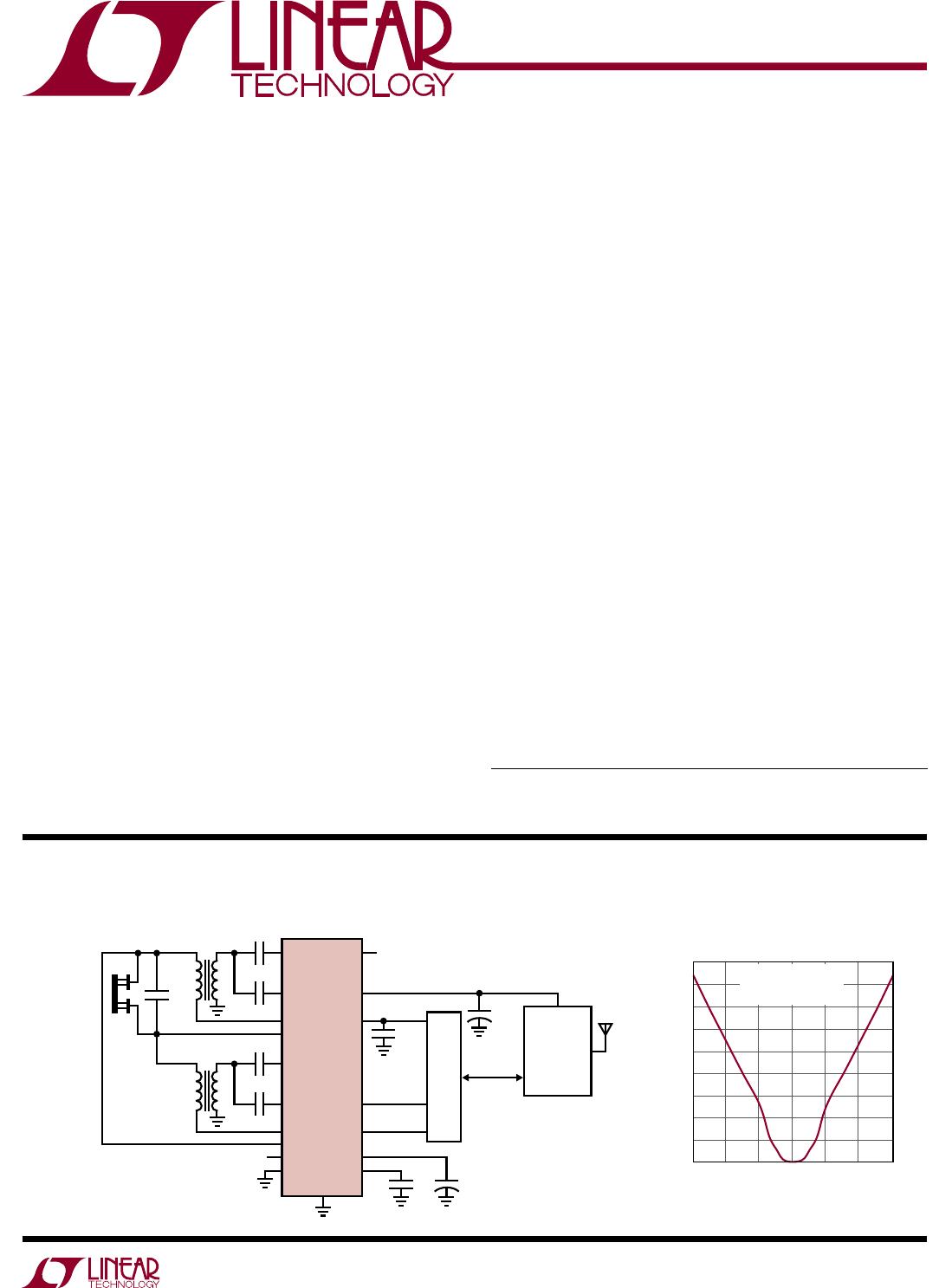
Typical applicaTion
FeaTures DescripTion
Auto-Polarity, Ultralow
Voltage Step-Up Converter
and Power Manager
The LT C
®
3109 is a highly integrated DC/DC converter ideal
for harvesting surplus energy from extremely low input
voltage sources such as TEGs (thermoelectric genera
-
tors) and thermopiles. Its unique, proprietary autopolarity
topology* allows it to operate from input voltages as low
as 30mV, regardless of polarity.
Using two compact step-up transformers and external
energy storage elements, the LTC3109 provides a com
-
plete power management solution for wireless sensing
and data acquisition. The 2.2V LDO can power an external
microprocessor, while the main output can be programmed
to one of four fixed voltages. The power good indicator
signals that the main output is within regulation. A second
output can be enabled by the host. A storage capacitor (or
battery) can also be charged to provide power when the
input voltage source is unavailable. Extremely low quies
-
cent current and high efficiency maximizes the harvested
energy available for the application.
The LTC3109 is available in a small, thermally enhanced
20-lead (4mm × 4mm) QFN package and a 20-lead SSOP
package.
V
OUT
Current vs TEG Voltage
applicaTions
n
Operates from Inputs as Low as ±30mV
n
Less Than ±1°C Needed Across TEG to Harvest
Energy
n
Proprietary Auto-Polarity Architecture
n
Complete Energy Harvesting Power Management
System
– Selectable V
OUT
of 2.35V, 3.3V, 4.1V or 5V
– 2.2V, 5mA LDO
– Logic-Controlled Output
– Energy Storage Capability for Operation During
Power Interruption
n
Power Good Indicator
n
Uses Compact Step-up Transformers
n
Small, 20-lead (4mm × 4mm) QFN Package or
20-Lead SSOP
n
Remote Sensor and Radio Power
n
HVAC Systems
n
Automatic Metering
n
Building Automation
n
Predictive Maintenance
n
Industrial Wireless Sensing
L, LT, LTC, LTM, Linear Technology and the Linear logo are registered trademarks of Linear
Technology Corporation. All other trademarks are the property of their respective owners.
*Patent pending.
GND
1µF
5.25V
2.2V
LTC3109
3.3V
C
STORE
3109 TA01a
C1A
1nF
2.2µF
470pF
47µF
1nF
470pF
1:100
TEG
(THERMOELECTRIC GENERATOR)
±30mV TO ±500mV
1:100
V
OUT2
C2A
C1B
C2B
SWB
V
INB
VS1
VS2
SWA
V
INA
V
OUT
VLDO
PG00D
V
OUT2_EN
VSTOREVAUX
VAUX
+
470µF
OPTIONAL SWITCHED OUTPUT FOR SENSORS
+
µP
LOW POWER
RADIO
SENSOR(S)
V
TEG
(mV)
–300
0
I
VOUT
(µA)
100
300
400
500
100
900
3109 TA01b
200
–100
–200
200
0 300
600
700
800
1:100 TRANSFORMERS
C1A = C1B = 1nF
V
OUT
= 3.3V
LTC3109
2
3109fb
For more information www.linear.com/LTC3109
absoluTe MaxiMuM raTings
SWA, SWB, V
INA
, V
INB
Voltage .................... 0.3V to 2V
C1A, C1B Voltage ......................................... 0.3V to 6V
C2A, C2B Voltage (Note 6) .............................. 8V to 8V
V
OUT2
, V
OUT2_EN
.......................................... 0.3V to 6V
VS1, VS2, V
OUT
, PGOOD .............................. 0.3V to 6V
(Note 1)
orDer inForMaTion
LEAD FREE FINISH TAPE AND REEL PART MARKING* PACKAGE DESCRIPTION TEMPERATURE RANGE
LTC3109EUF#PBF LTC3109EUF#TRPBF 3109 20-Lead (4mm × 4mm) Plastic QFN –40°C to 125°C
LTC3109IUF#PBF LTC3109IUF#TRPBF 3109 20-Lead (4mm × 4mm) Plastic QFN –40°C to 125°C
LTC3109EGN#PBF LTC3109EGN#TRPBF LTC3109GN 20-Lead Plastic SSOP –40°C to 125°C
LTC3109IGN#PBF LTC3109IGN#TRPBF LTC3109GN 20-Lead Plastic SSOP –40°C to 125°C
Consult LTC Marketing for parts specified with wider operating temperature ranges. *The temperature grade is identified by a label on the shipping container.
Consult LTC Marketing for information on non-standard lead based finish parts.
For more information on lead free part marking, go to: http://www.linear.com/leadfree/
For more information on tape and reel specifications, go to: http://www.linear.com/tapeandreel/
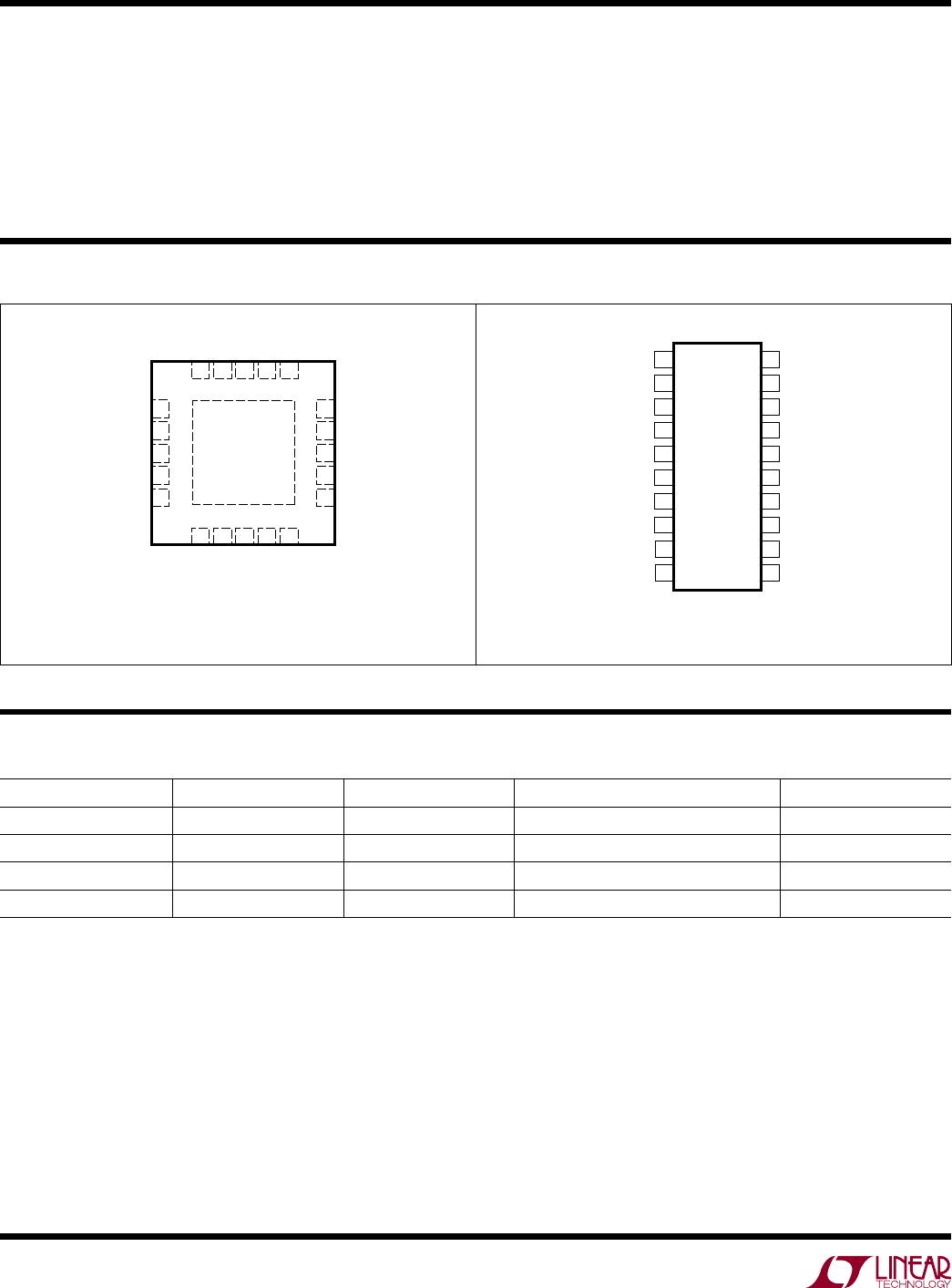
20 19 18 17 16
6 7 8
TOP VIEW
21
GND
UF PACKAGE
20-LEAD (4mm × 4mm) PLASTIC QFN
9 10
5
4
3
2
1
11
12
13
14
15
VSTORE
VAUX
V
OUT
V
OUT2
V
OUT2_EN
SWA
V
INA
V
INB
SWB
GND
VS2
VS1
C1A
C2A
GND
PGOOD
VLDO
GND
C1B
C2B
T
JMAX
= 125°C, θ
JA
= 37°C/W
EXPOSED PAD (PIN 21) IS GND (Note 5)
GN PACKAGE
20-LEAD PLASTIC SSOP
1
2
3
4
5
6
7
8
9
10
TOP VIEW
20
19
18
17
16
15
14
13
12
11
VS1
VS2
VSTORE
VAUX
V
OUT
V
OUT2
V
OUT2_EN
PGOOD
VLDO
GND
C1A
C2A
GND
SWA
V
INA
V
INB
SWB
GND
C2B
C1B
T
JMAX
= 125°C, θ
JA
= 90°C/W
pin conFiguraTion
VLDO, VSTORE ............................................ 0.3V to 6V
VAUX ...................................................... 15mA Into V
AUX
Operating Junction Temperature Range
(Note 2) .................................................. 40°C to 125°C
Storage Temperature Range .................. 65°C to 125°C
LTC3109
3
3109fb
For more information www.linear.com/LTC3109
elecTrical characTerisTics
Note 1: Stresses beyond those listed under Absolute Maximum Ratings
may cause permanent damage to the device. Exposure to any Absolute
Maximum Rating condition for extended periods may affect device
reliability and lifetime.
Note 2: The LTC3109 is tested under pulsed load conditions such that
T
J
≈ T
A
. The LTC3109E is guaranteed to meet specifications from
The l denotes the specifications which apply over the full operating
junction temperature range, otherwise specifications are for T
A
= 25°C (Note 2). VAUX = 5V unless otherwise noted.
PARAMETER CONDITIONS MIN TYP MAX UNITS
Minimum Start-Up Voltage Using 1:100 Transformer Turns Ratio, VAUX = 0V ±30 ±50 mV
No-Load Input Current Using 1:100 Transformer Turns Ratios,
V
IN
= 30mV, V
OUT2_EN
= 0V, All Outputs Charged
and in Regulation
6 mA
Input Voltage Range Using 1:100 Transformer Turns Ratios
l
V
STARTUP
±500 mV
Output Voltage VS1 = VS2 = GND
VS1 = VAUX, VS2 = GND
VS1 = GND, VS2 = VAUX
VS1 = VS2 = VAUX
l
l
l
l
2.30
3.234
4.018
4.875
2.350
3.300
4.100
5.000
2.40
3.366
4.182
5.10
V
V
V
V
VAUX Quiescent Current No Load, All Outputs Charged 7 10 µA
VAUX Clamp Voltage Current Into VAUX = 5mA
l
5.0 5.25 5.55 V
V
OUT
Quiescent Current V
OUT
= 3.3V, V
OUT2_EN
= 0V 0.2 µA
V
OUT
Current Limit V
OUT
= 0V
l
6 15 26 mA
N-Channel MOSFET On-Resistance C2B = C2A = 5V (Note 3) Measured from V
INA
or
SWA, V
INB
or SWB to GND
0.35 Ω
LDO Output Voltage 0.5mA Load On V
LDO
l
2.134 2.2 2.30 V
LDO Load Regulation For 0mA to 2mA Load 0.5 1 %
LDO Line Regulation For V
AUX
from 2.5V to 5V 0.05 0.2 %
LDO Dropout Voltage I
LDO
= 2mA
l
100 200 mV
LDO Current Limit V
LDO
= 0V
l
5 12 mA
VSTORE Leakage Current VSTORE = 5V 0.1 0.3 µA
VSTORE Current Limit VSTORE = 0V
l
6 15 26 mA
V
OUT2
Leakage Current V
OUT2
= 0V, V
OUT2_EN
= 0V 50 nA
VS1, VS2 Threshold Voltage
l
0.4 0.85 1.2 V
VS1, VS2 Input Current V
S1
= V
S2
= 5V 1 50 nA
PGOOD Threshold (Rising) Measured Relative to the V
OUT
Voltage –7.5 %
PGOOD Threshold (Falling) Measured Relative to the V
OUT
Voltage –9 %
PGOOD V
OL
Sink Current = 100µA 0.12 0.3 V
PGOOD V
OH
Source Current = 0 2.1 2.2 2.3 V
PGOOD Pull-Up Resistance 1
V
OUT2_EN
Threshold Voltage V
OUT2_EN
Rising
l
0.4 1.0 1.3 V
V
OUT2_EN
Threshold Hysteresis 100 mV
V
OUT2_EN
Pull-Down Resistance 5
V
OUT2
Turn-On Time 0.5 µs
V
OUT2
Turn-Off Time (Note 3) 0.15 µs
V
OUT2
Current Limit V
OUT
= 3.3V
l
0.2 0.3 0.5 A
V
OUT2
Current Limit Response Time (Note 3) 350 ns
V
OUT2
P-Channel MOSFET On-Resistance V
OUT
= 5V (Note 3) 1.0 Ω
0°C to 85°C junction temperature. Specifications over the –40°C to
125°C operating junction temperature range are assured by design,
characterization and correlation with statistical process controls. The
LTC3109I is guaranteed over the full –40°C to 125°C operating junction
temperature range. Note that the maximum ambient temperature
is determined by specific operating conditions in conjunction with
LTC3109EUF#PBF

Mfr. #:
Manufacturer:
Analog Devices / Linear Technology
Description:
Switching Voltage Regulators Auto-Polarity, UltraLow Voltage Step-Up Converter and Power Manager
Lifecycle:
New from this manufacturer.
Delivery:
DHL FedEx Ups TNT EMS
Payment:
T/T Paypal Visa MoneyGram Western Union