LTC3109
10
3109fb
For more information www.linear.com/LTC3109
V
OUT
storage capacitor is still charging. In the event of a
step load on the LDO output, current can come from the
main V
OUT
reservoir capacitor. The LDO requires a 2.2µF
ceramic capacitor for stability. Larger capacitor values
can be used without limitation, but will increase the time
it takes for all the outputs to charge up. The LDO output
is current limited to 5mA minimum.
V
OUT
The main output voltage on V
OUT
is charged from the VAUX
supply, and is user-programmed to one of four regulated
voltages using the voltage select pins VS1 and VS2, ac
-
cording to Table 2. Although the logic-threshold voltage
for VS1 and VS2 is 0.85V typical, it is recommended that
they be tied to ground or VAUX.
Table 2
VS2 VS1 V
OUT
GND GND 2.35V
GND VAUX 3.3V
VAUX GND 4.1V
VAUX VAUX 5V
When the output voltage drops slightly below the regulated
value, the charging current will be enabled as long as VAUX
is greater than 2.5V. Once V
OUT
has reached the proper
value, the charging current is turned off. The resulting
ripple on V
OUT
is typically less than 20mV peak to peak
.
The internal programmable resistor divider, controlled by
VS1 and VS2, sets V
OUT
, eliminating the need for very
high value external resistors that are susceptible to noise
pickup and board leakages.
In a typical application, a reservoir capacitor (typically a
few hundred microfarads) is connected to V
OUT
. As soon
as VAUX exceeds 2.5V, the V
OUT
capacitor will begin to
charge up to its regulated voltage. The current available
to charge the capacitor will depend on the input voltage
and transformer turns ratio, but is limited to about 15mA
typical. Note that for very low input voltages, this current
may be in the range of 1µA to 1000µA.
PGOOD
A power good comparator monitors the V
OUT
voltage.
The PGOOD pin is an open-drain output with a weak pull-
up (1MΩ) to the LDO voltage. Once V
OUT
has charged
to within 7.5% of its programmed voltage, the PGOOD
output will go high. If V
OUT
drops more than 9% from its
programmed voltage, PGOOD will go low. The PGOOD
output is designed to drive a microprocessor or other
chip I/O and is not intended to drive a higher current load
such as an LED. The PGOOD pin can also be pulled low in
a wire-OR configuration with other circuitry.
V
OUT2
V
OUT2
is an output that can be turned on and off by the
host using the V
OUT2_EN
pin. When enabled, V
OUT2
is con-
nected to V
OUT
through a 1Ω P-channel MOSFET switch.
This output, controlled by a host processor, can be used
to power external circuits such as sensors and amplifiers,
that don’t have a low power “sleep” or shutdown capabil
-
ity. V
OUT2
can be used to power these circuits only when
they are needed.
Minimizing the amount of decoupling capacitance on
V
OUT2
enables it to be switched on and off faster, allow-
ing shorter pulse times and therefore smaller duty cycles
in applications such as a wireless sensor/transmitter. A
small V
OUT2
capacitor will also minimize the energy that
will be wasted in charging the capacitor every time V
OUT2
is enabled.
V
OUT2
has a current limiting circuit that limits the peak
current to 0.3A typical.
The V
OUT2
enable input has a typical threshold of 1V
with 100mV of hysteresis, making it logic compatible. If
V
OUT2_EN
(which has an internal 5M pull-down resistor)
is low, V
OUT2
will be off. Driving V
OUT2_EN
high will turn
on the V
OUT2
output.
Note that while V
OUT2_EN
is high, the current limiting cir-
cuitry for V
OUT2
draws an extra 8µA of quiescent current
from V
OUT
. This added current draw has a negligible effect
operaTion
(Refer to the Block Diagram)
LTC3109
11
3109fb
For more information www.linear.com/LTC3109
on the application and capacitor sizing, since the load on
the V
OUT2
output, when enabled, is likely to be orders of
magnitude higher than 8µA.
VSTORE
The VSTORE output can be used to charge a large storage
capacitor or rechargeable battery. Once V
OUT
has reached
regulation, the VSTORE output will be allowed to charge
up to the clamped VAUX voltage (5.25V typical). The
storage element on VSTORE can then be used to power
the system in the event that the input source is lost, or
is unable to provide the current demanded by the V
OUT
,
V
OUT2
and LDO outputs.
If VAUX drops below VSTORE, the LTC3109 will automati
-
cally draw current from the storage element. Note that it
may take a long time to charge a large storage capacitor,
depending on the input energy available and the loading
on V
OUT
and VLDO.
Since the maximum charging current available at the
VSTORE output is limited to about 15mA, it can safely be
used to trickle charge NiCd or NiMH batteries for energy
storage when the input voltage is lost.
Note that VSTORE is not intended to supply high pulse
load currents to V
OUT
. Any pulse load on V
OUT
must be
handled by the V
OUT
reservoir capacitor.
Short-Circuit Protection
All outputs of the LTC3109 are current limited to protect
against short circuits to ground.
Output Voltage Sequencing
A timing diagram showing the typical charging and voltage
sequencing of the outputs is shown in Figure 1. Note that
the horizontal (time) axis is not to scale, and is used for
illustration purposes to show the relative order in which
the output voltages come up.
operaTion
(Refer to the Block Diagram)
5.0
VSTORE
PGOOD
V
OUT
VLDO
3.0
2.0
1.0
0
3.0
2.0
1.0
0
2.5
0
5.0
2.5
0
0 10 20 30 40
TIME (ms)
3109 F01
50 60 70 80
5.0
2.5
VOLTAGE (V)
0
VAUX
Figure 1. Output Voltage Sequencing
(with V
OUT
Programmed for 3.3V). Time Not to Scale
LTC3109
12
3109fb
For more information www.linear.com/LTC3109
applicaTions inForMaTion
INTRODUCTION
The LTC3109 is designed to gather energy from very low
input voltage sources and convert it to usable output
voltages to power microprocessors, wireless transmit
-
ters and analog sensors. Its architecture is specifically
tailored to applications where the input voltage polarity is
unknown, or can change. This “auto-polarity” capability
makes it ideally suited to energy harvesting applications
using a TEG whose temperature differential may be of
either polarity.
Applications such as wireless sensors typically require
much more peak power, and at higher voltages, than
the input voltage source can produce. The LTC3109 is
designed to accumulate and manage energy over a long
period of time to enable short power pulses for acquiring
and transmitting data. The pulses must occur at a low
enough duty cycle that the total output energy during the
pulse does not exceed the average source power integrated
over the accumulation time between pulses. For many
applications, this time between pulses could be seconds,
minutes or hours.
The PGOOD signal can be used to enable a sleeping
microprocessor or other circuitry when V
OUT
reaches
regulation, indicating that enough energy is available for
a transmit pulse.
INPUT VOLTAGE SOURCES
The LTC3109 can operate from a number of low input
voltage sources, such as Peltier cells (thermoelectric
generators), or low level AC sources. The minimum input
voltage required for a given application will depend on the
transformer turns ratios, the load power required, and the
internal DC resistance (ESR) of the voltage source. Lower
ESR sources will allow operation from lower input voltages,
and provide higher output power capability.
For a given transformer turns ratio, there is a maximum
recommended input voltage to avoid excessively high
secondary voltages and power dissipation in the shunt
regulator. It is recommended that the maximum input
voltage times the turns ratio be less than 50.
Note that a low ESR decoupling capacitor may be required
across a DC input source to prevent large voltage droop and
ripple caused by the source’s ESR and the peak primary
switching current (which can reach hundreds of milliamps).
Since the input voltage may be of either polarity, a ceramic
capacitor is recommended.
PELTIER CELL (THERMOELECTRIC GENERATOR)
A Peltier cell is made up of a large number of series-con
-
nected P-N junctions, sandwiched between two parallel
ceramic plates. Although Peltier cells are often used as
coolers by applying a DC voltage to their inputs, they will
also generate a DC output voltage, using the Seebeck effect,
when the two plates are at different temperatures.
When used in this manner, they are referred to as thermo-
electric generators (TEGs). The polarity of the output voltage
will depend on the polarity of the temperature differential
between the TEG plates. The magnitude of the output volt
-
age is proportional to the magnitude of the temperature
differential between the plates.
The low voltage capability of the LTC3109 design allows it
to operate from a typical TEG with temperature differentials
as low as 1°C of either polarity, making it ideal for harvest
-
ing energy in applications where a temperature difference
exists between two surfaces or between a surface and
the ambient temperature. The internal resistance (ESR)
of most TEGs is in the range of 1Ω to 5Ω, allowing for
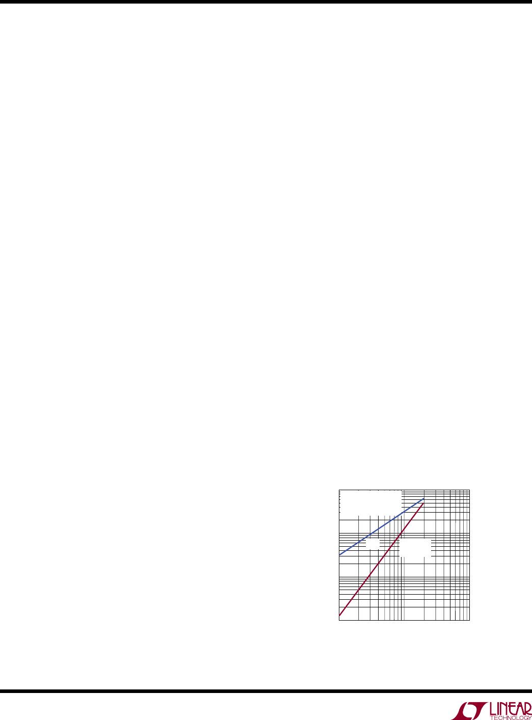
reasonable power transfer. The curves in Figure 2 show the
open-circuit output voltage and maximum power transfer
for a typical TEG with an ESR of 2Ω, over a 20°C range of
temperature differential (of either polarity).
dT (°C)
1
1
TEG V
OPEN-CIRCUIT
(mV)
TEG MAXIMUM P
OUT
– IDEAL (mW)
10
100
1000
0.1
1
10
100
10 100
3109 F02
TEG: 30mm SQUARE
127 COUPLES
R = 2Ω
V
OC
MAX P
OUT
(IDEAL)
Figure 2. Typical Performance of a Peltier Cell
Acting as a Power Generator (TEG)

LTC3109EUF#PBF

Mfr. #:
Manufacturer:
Analog Devices / Linear Technology
Description:
Switching Voltage Regulators Auto-Polarity, UltraLow Voltage Step-Up Converter and Power Manager
Lifecycle:
New from this manufacturer.
Delivery:
DHL FedEx Ups TNT EMS
Payment:
T/T Paypal Visa MoneyGram Western Union