LTC3109
16
3109fb
For more information www.linear.com/LTC3109
applicaTions inForMaTion
Note that there must be enough energy available from the
input voltage source for V
OUT
to recharge the capacitor
during the interval between load pulses (as discussed in
Design Example 1). Reducing the duty cycle of the load
pulse will allow operation with less input energy.
The VSTORE capacitor may be of very large value (thou
-
sands of microfarads or even Farads), to provide energy
storage at times when the input voltage is lost. Note that
this capacitor can charge all the way to the VAUX clamp
voltage of 5.25V typical (regardless of the settings for
V
OUT
), so be sure that the holdup capacitor has a work-
ing voltage rating of at least 5.5V at the temperature that
it will be used.
The VSTORE input is not designed to provide high pulse
load currents to V
OUT
. The current path from VSTORE to
V
OUT
is limited to about 26mA max.
The VSTORE capacitor can be sized using the following
formula:
C
STORE
7µA
+
I
Q
+
I
LDO
+
I
PULSE
t
PULSE
f
( )
( )
t
STORE
5.25 – V
OUT
where 7µA is the quiescent current of the LTC3109, I
Q
is
the load on V
OUT
in between pulses, I
LDO
is the load on
the LDO between pulses, I
PULSE
is the total load during the
pulse, t
PULSE
is the duration of the pulse, f is the frequency
of the pulses, t
STORE
is the total storage time required
and V
OUT
is the output voltage required. Note that for a
programmed output voltage of 5V, the VSTORE capacitor
cannot provide any beneficial storage time to V
OUT
.
To minimize losses and capacitor charge time, all capaci
-
tors used for V
OUT
and VSTORE should be low leakage.
See Table 6 for recommended storage capacitors.
Table 6. Recommended Storage Capacitors
VENDOR PART NUMBER/SERIES
AVX
www.avx.com
BestCap Series
TAJ and TPS Series Tantalum
Cap-XX
www.cap-xx.com
GZ Series
Cooper/Bussman
www.bussmann.com/3/PowerStor.html
KR Series
P Series
Vishay/Sprague
www.vishay.com/capacitors
Tantamount 592D
595D Tantalum
Note that storage capacitors requiring voltage balancing
resistors are not recommended due to the steady-state
current draw of the resistors.
PCB LAYOUT GUIDELINES
Due to the rather low switching frequency of the resonant
converter and the low power levels involved, PCB layout
is not as critical as with many other DC/DC converters.
There are however, a number of things to consider.
Due to the very low input voltages the circuit operates from,
the connections to V
IN
, the primary of the transformers
and the SW, V
IN
and GND pins of the LTC3109 should be
designed to minimize voltage drop from stray resistance,
and able to carry currents as high as 500mA. Any small
voltage drop in the primary winding conduction path will
lower efficiency and increase start-up voltage and capaci
-
tor charge time.
Also, due to the low charge currents available at the out
-
puts of the LTC3109, any sources of leakage current on
the output voltage pins must be minimized. An example
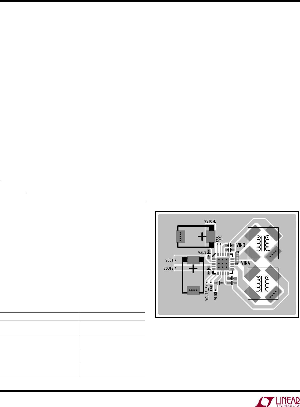
board layout is shown in Figure 4.
Figure 4. Example Component Placement for 2-Layer PC Board
(QFN Package). Note That VSTORE and VOUT Capacitor Sizes
are Application Dependent
LTC3109
17
3109fb
For more information www.linear.com/LTC3109
applicaTions inForMaTion
DESIGN EXAMPLE 1
This design example will explain how to calculate the
necessary reservoir capacitor value for V
OUT
in pulsed-
load applications, such as a wireless sensor/transmitter.
In these types of applications, the load is very small for a
majority of the time (while the circuitry is in a low power
sleep state), with pulses of load current occurring periodi
-
cally during a transmit burst.
The reservoir capacitor on V
OUT
supports the load during
the transmit pulse; the long sleep time between pulses
allows the LTC3109 to accumulate energy and recharge
the capacitor (either from the input voltage source or the
storage capacitor). A method for calculating the maximum
rate at which the load pulses can occur for a given output
current from the LTC3109 will also be shown.
In this example, V
OUT
is set to 3.3V, and the maximum
allowed voltage droop during a transmit pulse is 10%, or
0.33V. The duration of a transmit pulse is 5ms, with a total
average current requirement of 20mA during the pulse.
Given these factors, the minimum required capacitance
on V
OUT
is:
C
OUT
µF
( )
20mA 5ms
0.33V
= 303µF
Note that this equation neglects the effect of capacitor ESR
on output voltage droop. For ceramic capacitors and low
ESR tantalum capacitors, the ESR will have a negligible
effect at these load currents. However, beware of the voltage
coefficient of ceramic capacitors, especially those in small
case sizes. This greatly reduces the effective capacitance
when a DC bias is applied.
A standard value of 330µF could be used for C
OUT
in
this case. Note that the load current is the total current
draw on V
OUT
, V
OUT2
and VLDO, since the current for all
of these outputs must come from V
OUT
during a pulse.
Current contribution from the capacitor on VSTORE is not
considered, since it may not be able to recharge between
pulses. Also, it is assumed that the harvested charge
current from the LTC3109 is negligible compared to the
magnitude of the load current during the pulse.
To calculate the maximum rate at which load pulses can
occur, you must know how much charge current is avail
-
able from the LTC3109 V
OUT
pin given the input voltage
source being used. This number is best found empirically,
since there are many factors affecting the efficiency of the
converter. You must also know what the total load cur
-
rent is on V
OUT
during the sleep state (between pulses).
Note that this must include any losses, such as storage
capacitor leakage.
Let’s assume that the charge current available from the
LTC3109 is 150µA and the total current draw on V
OUT
and
VLDO in the sleep state is 17µA, including capacitor leakage.
We’ll also use the value of 330µF for the V
OUT
capacitor.
The maximum transmit rate (neglecting the duration of
the transmit pulse, which is very short compared to the
period) is then given by:
T =
330µF 0.33V
150µA 17µA
= 0.82sec or f
MAX
= 1.2Hz
Therefore, in this application example, the circuit can sup-
port a 5ms transmit pulse of 20mA every 0.82 seconds.
It can be seen that for systems that only need to transmit
every few seconds (or minutes or hours), the average
charge current required is extremely small, as long as
the sleep or standby current is low. Even if the available
charge current in the example above was only 21µA, if the
sleep current was only 5µA, it could still transmit a pulse
every seven seconds.
The following formula will allow you to calculate the time
it will take to charge the LDO output capacitor and the
V
OUT
capacitor the first time, from zero volts. Here again,
the charge current available from the LTC3109 must be
known. For this calculation, it is assumed that the LDO
output capacitor is 2.2µF:
t
LDO
=
2.2V 2.2µF
I
CHG
I
LDO
If there was 150µA of charge current available and a 5µA
load on the LDO (when the processor is sleeping), the time
for the LDO to reach regulation would be only 33ms.
LTC3109
18
3109fb
For more information www.linear.com/LTC3109
applicaTions inForMaTion
The time for V
OUT
to charge and reach regulation can be
calculated by the formula below, which assumes V
OUT
is
programmed to 3.3V and C
OUT
is 330µF:
t
VOUT
=
3.3V 330µF
I
CHG
I
VOUT
I
LDO
+ t
LDO
With 150µA of charge current available and 5µA of load on
both V
OUT
and VLDO, the time for V
OUT
to reach regula-
tion after the initial application of power would be 7.81
seconds.
DESIGN EXAMPLE 2
In most pulsed-load applications, the duration, magnitude
and frequency of the load current pulses are known and
fixed. In these cases, the average charge current required
from the LTC3109 to support the average load must be
calculated, which can be easily done by the following:
I
CHG
I
Q
+
I
PULSE
t
PULSE
T
where I
Q
is the sleep current supplied by V
OUT
and V
LDO
to the external circuitry in-between load pulses, including
output capacitor leakage, I
PULSE
is the total load current
during the pulse, t
PULSE
is the duration of the load pulse
and T is the pulse period (essentially the time between
load pulses).
In this example, I
Q
is 5µA, I
PULSE
is 100mA, t
PULSE
is 5ms
and T is one hour. The average charge current required
from the LTC3109 would be:
I
CHG
5µA +
100mA 0.005sec
3600sec
= 5.14µA
Therefore, if the LTC3109 has an input voltage that allows
it to supply a charge current greater than just 5.14µA, the
application can support 100mA pulses lasting 5ms every
hour. It can be seen that the sleep current of 5µA is the
dominant factor in this example, because the transmit
duty cycle is so small (0.00014%). Note that for a V
OUT
of 3.3V, the average power required by this application is
only 17µW (not including converter losses).
Keep in mind that the charge current available from the
LTC3109 has no effect on the sizing of the V
OUT
capacitor,
and the V
OUT
capacitor has no effect on the maximum
allowed pulse rate.

LTC3109EUF#PBF

Mfr. #:
Manufacturer:
Analog Devices / Linear Technology
Description:
Switching Voltage Regulators Auto-Polarity, UltraLow Voltage Step-Up Converter and Power Manager
Lifecycle:
New from this manufacturer.
Delivery:
DHL FedEx Ups TNT EMS
Payment:
T/T Paypal Visa MoneyGram Western Union