VS-ST303S12PFK0

VS-ST303SP Series
www.vishay.com
Vishay Semiconductors
Revision: 15-Mar-17
7
Document Number: 94375
For technical questions within your region: DiodesAmericas@vishay.com
, DiodesAsia@vishay.com, DiodesEurope@vishay.com
THIS DOCUMENT IS SUBJECT TO CHANGE WITHOUT NOTICE. THE PRODUCTS DESCRIBED HEREIN AND THIS DOCUMENT
ARE SUBJECT TO SPECIFIC DISCLAIMERS, SET FORTH AT www.vishay.com/doc?91000
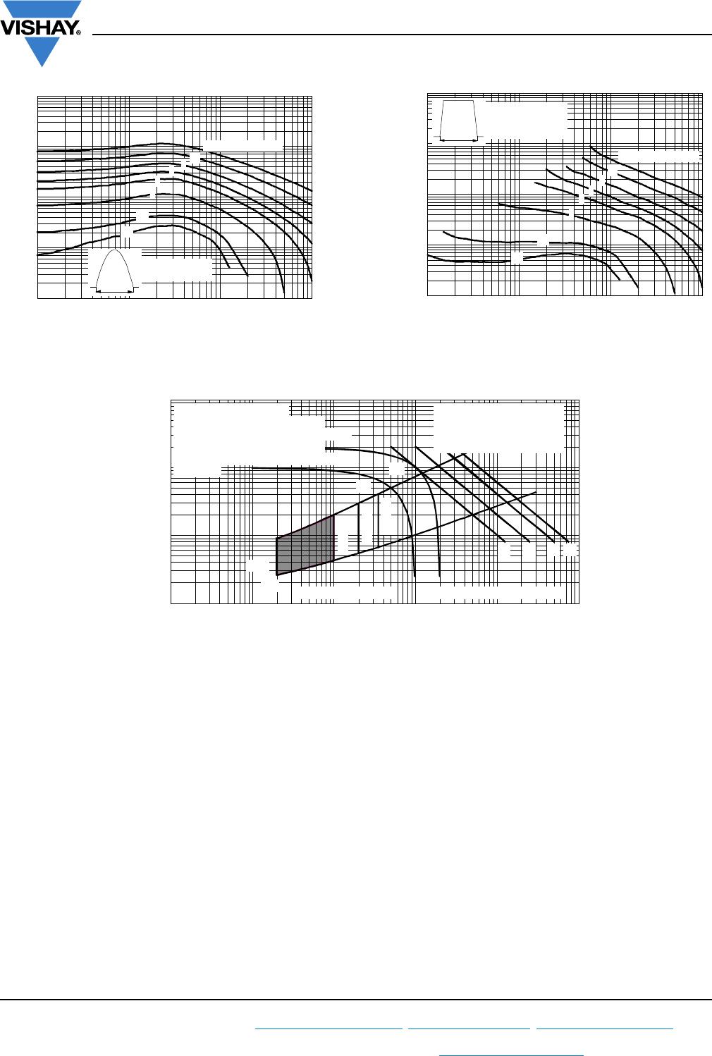
Fig. 14 - Maximum On-State Energy Power Loss Characteristics
Fig. 15 - Gate Characteristics
1E1
1E2
1E3
1E4
1E5
1 E1 1 E2 1 E3 1 E4
Pulse Ba sew id t h ( µs)
20 joules p er pulse
2
1
Peak On-state Current (A)
0.5
10
5
3
0.4
ST3 0 3 S Se r i e s
Sinusoid al p ulse
tp
1E1 1E2 1E3 1E4
Pulse Ba sew id t h ( µ s)
20 joule s p er p ulse
2
1
0.5
10
5
ST3 0 3 S Se r i e s
Rectangular pulse
di/dt = 50A/µs
tp
3
0.4
0.1
1
10
100
0.001 0.01 0.1 1 10 100
VGD
IGD
(b)
(a)
Tj = 2 5 ° C
Tj = 1 2 5 ° C
Tj= - 4 0 ° C
(1)
(2)
Instant a neous Ga te Current (A)
In st a n t a n e o us G a t e V o l t a g e ( V )
Rectangular gate pulse
a) Recommended load line for
b) Recommended load line for
<=30% rated di/ dt : 10V, 10ohms
rated d i/ dt : 20V, 10ohms; tr<=1 µs
tr<=1 µs
(1) PGM = 10W, tp = 20ms
(2) PGM = 20W, tp = 10ms
(3) PGM = 40W, tp = 5ms
(4) PGM = 60W, tp = 3.3ms
(3)
De vic e: ST303S Series
(4)
Frequency Limited by PG(AV)
VS-ST303SP Series
www.vishay.com
Vishay Semiconductors
Revision: 15-Mar-17
8
Document Number: 94375
For technical questions within your region: DiodesAmericas@vishay.com
, DiodesAsia@vishay.com, DiodesEurope@vishay.com
THIS DOCUMENT IS SUBJECT TO CHANGE WITHOUT NOTICE. THE PRODUCTS DESCRIBED HEREIN AND THIS DOCUMENT
ARE SUBJECT TO SPECIFIC DISCLAIMERS, SET FORTH AT www.vishay.com/doc?91000
ORDERING INFORMATION TABLE
LINKS TO RELATED DOCUMENTS
Dimensions www.vishay.com/doc?95080
- Thyristor
- Essential part number
- 3 = fast turn-off
- S = compression bonding stud
- Voltage code x 100 = V
RRM
- P = stud base 3/4" 16UNF-2A
- Reapplied dV/dt code (for t
q
test condition)
-t
q
code
- 0 = eyelet terminals
1 = fast-on terminals
dV/dt - t
q
combinations available
dV/dt (V/µs) 200
10
15
t
q
(µs)
FN
FL
20 FK
20
FK
up to 800 V
t
q
(µs)
only for
1000/1200 V
(see Voltage Ratings table)
(gate and auxiliary cathode leads)
Device code
51 32 4 6 7 8 9 10 11
ST 30 3 S 12 P F K 0 P
1
- Vishay Semiconductors product
11
- None = standard production
- P = lead (Pb)-free
VS-
2
3
4
5
6
7
9
10
8
Document Number: 95080 For technical questions, contact: indmodules@vishay.com
www.vishay.com
Revision: 02-Aug-07 1
TO-209AE (TO-118)
Outline Dimensions
Vishay Semiconductors
DIMENSIONS in millimeters (inches)
Note
(1)
For metric device: M24 x 1.5 - length 21 (0.83) maximum
Red cathode
Red silicon rubber
10.5 (0.41) NOM.
245 (9.65) ± 10 (0.39)
White gate
4.3 (0.17) DIA.
Ceramic housing
White shrink
47 (1.85)
MAX.
245 (9.65)
255 (10.04)
38 (1.50)
MAX. DIA.
22 (0.87) MAX.
21 (0.82) MAX.
SW 45
Flexible leads
4.5 (0.18) MAX.
C.S. 50 mm
2
(0.078 s.i.)
Red shrink
49 (1.92) MAX.
3/4"16 UNF-2A
(1)
27.5 (1.08)
MAX.
Fast-on terminals
AMP. 280000-1
REF-250
9.5 (0.37) MIN.
22 (0.86) MIN.

VS-ST303S12PFK0

Mfr. #:
Manufacturer:
Vishay Semiconductors
Description:
SCR Modules Thyristors - TO-118 COMP RND-e3
Lifecycle:
New from this manufacturer.
Delivery:
DHL FedEx Ups TNT EMS
Payment:
T/T Paypal Visa MoneyGram Western Union