DG9408E, DG9409E
www.vishay.com
Vishay Siliconix
S16-1452-Rev. A, 25-Jul-16
1
Document Number: 75375
For technical questions, contact: analogswitchtechsupport@vishay.com
THIS DOCUMENT IS SUBJECT TO CHANGE WITHOUT NOTICE. THE PRODUCTS DESCRIBED HEREIN AND THIS DOCUMENT
ARE SUBJECT TO SPECIFIC DISCLAIMERS, SET FORTH AT www.vishay.com/doc?91000
3.2 , Fast Switching Speed, +12 V / +5 V / +3 V / ± 5 V,
4- / 8-Channel Analog Multiplexers
DESCRIPTION
The DG9408E, DG9409E uses BiCMOS wafer fabrication
technology that allows the DG9408E, DG9409E to operate
on single and dual supplies. Single supply voltage
ranges from 3 V to 16 V while dual supply operation is
recommended with ± 3 V to ± 8 V.
The DG9408E is an 8-channel single-ended analog
multiplexer designed to connect one of eight inputs to a
common output as determined by a 3-bit binary address
(A
0
, A
1
, A
2
). The DG9409E is a dual 4-channel differential
analog multiplexer designed to connect one of four
differential inputs to a common dual output as determined
by its 2-bit binary address (A
0
, A
1
). Break-before-make
switching action to protect against momentary crosstalk
between adjacent channels.
As a committed partner to the community and the
environment, Vishay Siliconix manufactures this product
with lead (Pb)-free device terminations. The DG9408E,
DG9409E are offered in a QFN package that has a
nickel-palladium-gold device terminations and is
represented by the lead (Pb)-free “-E4” suffix. The
nickel-palladium-gold device terminations meet all the
JEDEC
®
standards for reflow and MSL ratings.
FEATURES
3 V to 16 V single supply or ± 3 V to ± 8 V dual
supply operation
Low on-resistance - R
ON
: 3.2 typ.
Fast switching: t
ON
- 36 ns, t
OFF
- 24 ns
Break-before-make guaranteed
Low leakage
TTL, CMOS, LV logic (3 V) compatible
2500 V ESD protection (HBM)
Material categorization: for definitions of compliance
please see www.vishay.com/doc?99912
BENEFITS
Fast switching speed
Low switch resistance
Wide operation voltage range
Simple logic interface
APPLICATIONS
Automatic test equipment
Process control and automation
Data acquisition systems
Meters and instruments
Medical and healthcare systems
Communication systems
Audio and video signal routing
Relay replacement
Battery powered systems
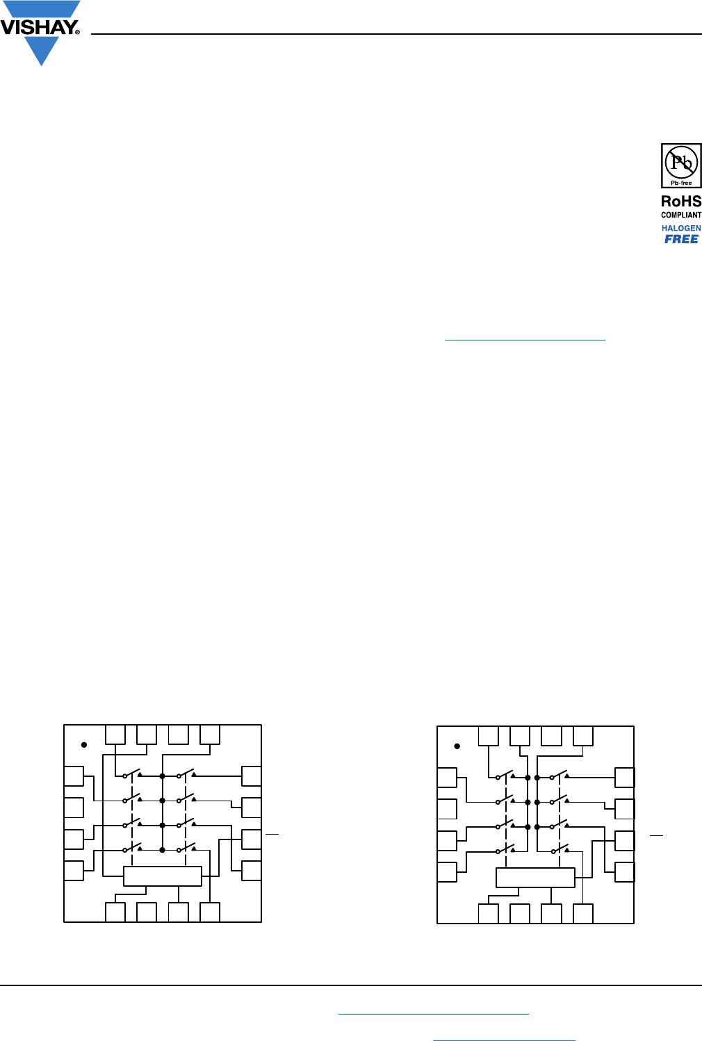
FUNCTIONAL BLOCK DIAGRAM AND PIN CONFIGURATION
Note
QFN16 package central exposed pad has no electrical connection inside the chip. It can be connected GND, V+, V-, or left floating.
49
GND S
2a
S
4b
S
3b
S
3a
EN
S
2b
S
1a
1
2
3
12
11
10
567
8
16 15 14 13
A
0
V+ A
1
S
4a
S
1b
D
b
V- D
a
Decoder / driver
Top view
DG9409E
QFN16
5
GND S
6
S
4
S
3
S
7
EN
S
2
S
5
1
2
3
12
11
10
49
5678
16 15 14 13
A
0
V+ A
1
S
8
S
1
A
2
V- D
Decoder / driver
Top view
DG9408E
QFN16
DG9408E, DG9409E
www.vishay.com
Vishay Siliconix
S16-1452-Rev. A, 25-Jul-16
2
Document Number: 75375
For technical questions, contact: analogswitchtechsupport@vishay.com
THIS DOCUMENT IS SUBJECT TO CHANGE WITHOUT NOTICE. THE PRODUCTS DESCRIBED HEREIN AND THIS DOCUMENT
ARE SUBJECT TO SPECIFIC DISCLAIMERS, SET FORTH AT www.vishay.com/doc?91000
TRUTH TABLE AND ORDERING INFORMATION
X = do not care
For low and high voltage levels for V
AX
and V
EN
consult “Digital Control” parameters for specific V+ operation. See specifications
tables for:
Single supply 12 V
Dual supply V+ = 5 V, V- = -5 V
Single supply 5 V
Single supply 3 V
Notes
a. Signals on SX, DX or INX exceeding V+ or V- will be clamped by internal diodes. Limit forward diode current to maximum current ratings.
b. All leads soldered or welded to PC board.
c. Derate 23.5 mW/°C above 70 °C.
d. Manual soldering with soldering iron is not recommended for leadless components. The QFN is a leadless package. The end of the lead
terminal is exposed copper (not plated) as a result of the singulation process in manufacturing. A solder fillet at the exposed copper lip
cannot be guaranteed and is not required to ensure adequate bottom side solder interconnection.
Stresses beyond those listed under “Absolute Maximum Ratings” may cause permanent damage to the device. These are stress ratings only, and functional operation
of the device at these or any other conditions beyond those indicated in the operational sections of the specifications is not implied. Exposure to absolute maximum
rating conditions for extended periods may affect device reliability.
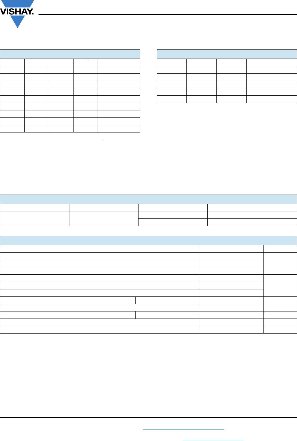
TRUTH TABLE DG9408E
A
2
A
1
A
0
EN ON SWITCH
XXX1 None
0000 1
0010 2
0100 3
0110 4
1000 5
1010 6
1100 7
1110 8
TRUTH TABLE DG9409E
A
1
A
0
EN ON SWITCH
XX1 None
000 1
010 2
100 3
110 4
ORDERING INFORMATION
TEMP. RANGE PACKAGE PART NUMBER MIN. ORDER / PACK. QUANTITY
-40 °C to +85 °C
16-pin QFN (4 mm x 4 mm)
(variation 1)
DG9408EDN-T1-GE4 Tape and reel, 2500 units
DG9409EDN-T1-GE4 Tape and reel, 2500 units
ABSOLUTE MAXIMUM RATINGS (T
A
= 25 °C, unless otherwise noted)
PARAMETER LIMIT UNIT
Voltage referenced V+ to V- -0.3 to +18
VGND to V- 18
Digital inputs
a
, V
S
, V
D
(V-) - 0.3 to (V+) + 0.3
Current (any terminal except S or D) 30
mAContinuous current, S or D 100
Peak current, S or D (pulsed at 1 ms, 10 % duty cycle max.) 200
Package solder reflow conditions (lead (Pb)-free assembly)
d
16-pin (4 x 4 mm) QFN 260 +0 / -5
°C
Storage temperature -65 to +150
Power dissipation (package)
b
, (T
A
= 70 °C) 16-pin (4 x 4 mm) QFN
c
1880 mW
ESD human body model (HBM), per ANSI / ESDA / JEDEC
®
JS-001 2500 V
Latch up current, per JESD78 400 mA
DG9408E, DG9409E
www.vishay.com
Vishay Siliconix
S16-1452-Rev. A, 25-Jul-16
3
Document Number: 75375
For technical questions, contact: analogswitchtechsupport@vishay.com
THIS DOCUMENT IS SUBJECT TO CHANGE WITHOUT NOTICE. THE PRODUCTS DESCRIBED HEREIN AND THIS DOCUMENT
ARE SUBJECT TO SPECIFIC DISCLAIMERS, SET FORTH AT www.vishay.com/doc?91000
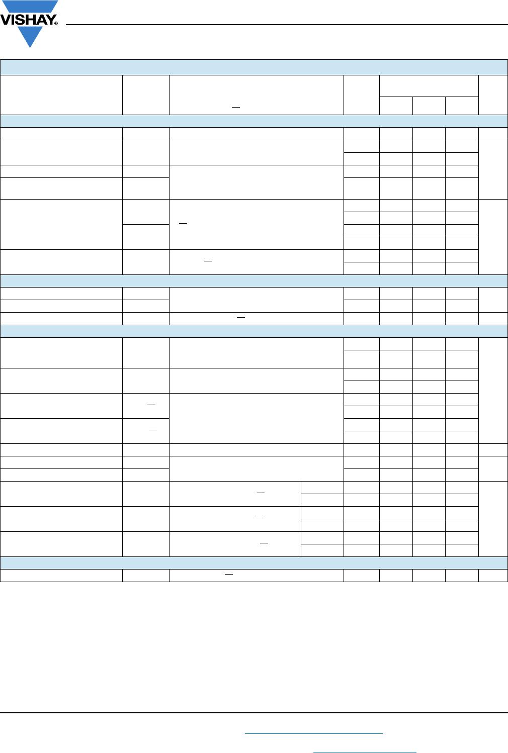
SPECIFICATIONS (Single Supply 12 V)
PARAMETER SYMBOL
TEST CONDITIONS
UNLESS OTHERWISE SPECIFIED
V+ = 12 V, ± 10 %, V- = 0 V
V
A
, V
EN
= 0.8 V or 2.4 V
f
TEMP.
b
LIMITS
-40 °C to +85 °C
UNIT
MIN.
c
TYP.
d
MAX.
c
Analog Switch
Analog signal range
e
V
ANALOG
Full 0 - 12 V
On-resistance R
ON
V+ = 10.8 V, V
D
= 2 V or 9 V, I
S
= 50 mA
sequence each switch on
Room - 3.2 7
Full - 7.5
R
ON
match between channels
g
R
ON
V+ = 10.8 V, V
D
= 2 V or 9 V, I
S
= 50 mA
Room - - 3.6
On-resistance flatness
i
R
ON
flatness
Room - - 8
Switch off leakage current
I
S(off)
V
EN
= 2.4 V, V
D
= 11 V or 1 V, V
S
= 1 V or 11 V
Room -2 - 2
nA
Full -15 - 15
I
D(off)
Room -2 - 2
Full -15 - 15
Channel on leakage current I
D(on)
V
EN
= 0 V, V
S
= V
D
= 1 V or 11 V
Room -2 - 2
Full -15 - 15
Digital Control
Logic high input voltage V
INH
Full 2.4 - -
V
Logic low input voltage V
INL
Full - - 0.8
Input current I
IN
V
AX
= V
EN
= 2.4 V or 0.8 V Full -1 - 1 μA
Dynamic Characteristics
Transition time t
TRANS
V
S1
= 8 V, V
S8
= 0 V, (DG9408E)
V
S1b
= 8 V, V
S4b
= 0 V, (DG9409E)
see fig. 2
Room - 40 71
ns
Full - - 75
Break-before-make time t
BBM
V
S(all)
= V
DA
= 5 V
see fig. 4
Room 2 20 -
Full - - -
Enable turn-on time t
ON(EN)
V
AX
= 0 V, V
S1
= 5 V (DG9408E)
V
AX
= 0 V, V
S1b
= 5 V (DG9409E)
see fig. 3
Room - 36 70
Full - - 75
Enable turn-off time t
OFF(EN)
Room - 24 44
Full - - 46
Charge injection
e
QC
L
= 1 nF, V
GEN
= 0 V, R
GEN
= 0 Room - 4.5 - pC
Off isolation
e, h
OIRR
f = 100 kHz, R
L
= 1 k
Room - -83 -
dB
Crosstalk
e
X
TALK
Room - -89 -
Source off capacitance
e
C
S(off)
f = 1 MHz, V
S
= 0 V, V
EN
= 2.4 V
DG9408E Room - 17 -
pF
DG9409E Room - 16 -
Drain off capacitance
e
C
D(off)
f = 1 MHz, V
D
= 0 V, V
EN
= 2.4 V
DG9408E Room - 134 -
DG9409E Room - 67 -
Drain on capacitance
e
C
D(on)
f = 1 MHz, V
D
= 0 V, V
EN
= 0 V
DG9408E Room - 154 -
DG9409E Room - 86 -
Power Supplies
Power supply current I+ V
EN
= V
A
= 0 V or V+ Room - - 1 μA

DG9409EDN-T1-GE4

Mfr. #:
Manufacturer:
Vishay / Siliconix
Description:
Multiplexer Switch ICs Dual 4-Ch Diffrntial Multiplexer 3-16V
Lifecycle:
New from this manufacturer.
Delivery:
DHL FedEx Ups TNT EMS
Payment:
T/T Paypal Visa MoneyGram Western Union

Products related to this Datasheet