Expand menu
Hello, Sign in
My Account
0
Cart
Home
Products
Sensors
Semiconductors
Passive Components
Connectors
Power
Electromechanical
Optoelectronics
Circuit Protection
Integrated Circuits - ICs
Main Products
Manufacturers
Blog
Services
About OMO
About Us
Contact Us
Check Stock
DG9409EDN-T1-GE4
P1-P3
P4-P6
P7-P9
P10-P12
P13-P15
DG9408E, DG9409E
www.vishay.com
Vishay Silicon
ix
S16-1452-Rev
. A, 25-Jul-16
10
Document Number: 75375
For technical questi
ons, contact:
analogswitchtechsupport@vishay
.com
THIS DOCUMENT IS SU
BJECT TO CHANGE WI
THOUT NOTICE. THE
PRODUCTS DESCRI
BED HEREIN AND THIS D
OCUMENT
ARE SUBJECT TO S
PECIFIC DISCLAIME
RS, SET FORTH A
T
www
.vishay
.com/doc?91000
TYPICAL CHAR
ACTERISTICS
(25 °C,
unless otherwise noted)
Capacitance vs. An
alog Voltage
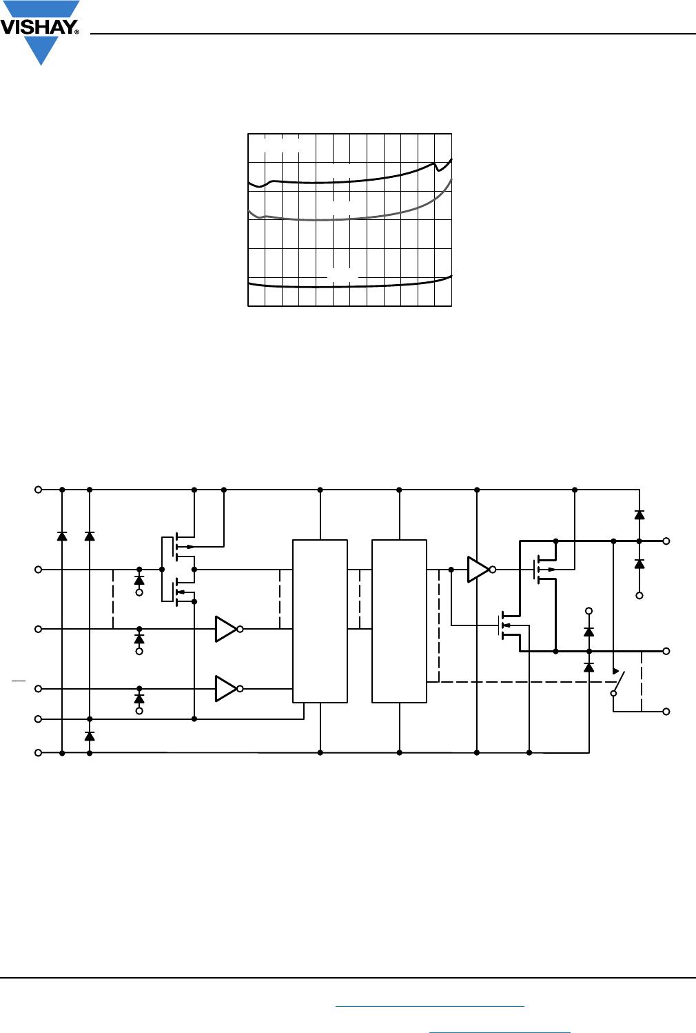
SCHEMATIC DIAGRAM
(Typical C
hannel)
Fig. 1 -
10
100
1000
10000
0
20
40
60
80
100
120
0123456789
1
0
1
1
1
2
Axis Title
1st line
2nd line
2nd line
Capacitance (pF)
V
ANALOG
(V)
2nd line
DG9409E
C
S(OFF)
C
D(ON)
C
D(OFF)
EN
A
0
S
1
D
V+
S
n
V-
Decode/
Drive
Level
Shift
V-
V+
A
X
GND
V-
V-
V-
DG9408E, DG9409E
www.vishay.com
Vishay Silicon
ix
S16-1452-Rev
. A, 25-Jul-16
11
Document Number: 75375
For technical questi
ons, contact:
analogswitchtechsupport@vishay
.com
THIS DOCUMENT IS SU
BJECT TO CHANGE WI
THOUT NOTICE. THE
PRODUCTS DESCRI
BED HEREIN AND THIS D
OCUMENT
ARE SUBJECT TO S
PECIFIC DISCLAIME
RS, SET FORTH A
T
www
.vishay
.com/doc?91000
TEST CIRCUITS
Fig. 2 - Transition Tim
e
Fig. 3 - Enable Switc
hing Time
A
1
A
0
A
2
A
1
A
0
V+
V-
V+
V-
GND
D
35 pF
V
O
S
1
S
2
- S
7
S
8
50
Ω
300
Ω
V
S8
V
S1
V+
V-
V+
V-
GND
35 pF
V
O
S
1b
S
1a
- S
4a
, D
a
S
4b
300
Ω
D
b
Logic
Input
Switch
Output
V
S8
V
O
t
TRANS
t
r
< 5 ns
t
f
< 5 ns
S
8
ON (DG9408)
or
S
4
ON (DG9409)
S
1
ON
t
TRANS
50 %
V
S1
50 %
90 %
90 %
3 V
0 V
DG9408E
DG9409E
V
S4b
V
S1b
V
AX
50
Ω
EN
EN
Return to Specifications:
Single Supply 12 V
Dual Supply V+ = 5 V
,
V-
=
- 5
V
Single Supply 5 V
Single Supply 3 V
Logic
Input
Switch
Output
V
O
t
r
< 5 ns
t
f
< 5 ns
3 V
0 V
0 V
t
ON(EN
)
t
OFF(EN
)
50 %
90 %
90 %
V
O
S
1
S
2
- S
8
A
0
A
1
A
2
50
300
V
O
V+
GND
V-
D
35 pF
V-
V+
S
1b
S
1a
- S
4a
, D
a
S
2b
- S
4b
D
b
A
0
A
1
50
300
V
O
V+
GND
V-
35 pF
V-
DG9408E
DG9409E
V
S1
V+
V
S1
EN
EN
Return to Specifications:
Single Supply 12 V
Dual Supply V+ = 5 V
,
V- =
- 5
V
Single Supply 5 V
Single Supply 3 V
DG9408E, DG9409E
www.vishay.com
Vishay Silicon
ix
S16-1452-Rev
. A, 25-Jul-16
12
Document Number: 75375
For technical questi
ons, contact:
analogswitchtechsupport@vishay
.com
THIS DOCUMENT IS SU
BJECT TO CHANGE WI
THOUT NOTICE. THE
PRODUCTS DESCRI
BED HEREIN AND THIS D
OCUMENT
ARE SUBJECT TO S
PECIFIC DISCLAIME
RS, SET FORTH A
T
www
.vishay
.com/doc?91000
TEST CIRCUITS
Fig. 4 - Break-Be
fore-Make Interv
al
Fig. 5 - Charge Injection
Fig. 6 - Off Isolation
50 %
90 %
Logic
Input
Switch
Output
V
O
V
S
t
OPEN
t
r
< 5 ns
t
f
< 5 ns
0 V
3 V
0 V
V+
GND
V-
35 pF
V-
A
2
D
b
, D
All S and D
a
300
V
O
50
A
1
A
0
DG9408E
DG9409E
V
S1
EN
Return to Specifications:
Single Supply 12 V
Dual Supply V+ = 5 V
,
V-
=
- 5
V
Single Supply 5 V
Single Supply 3 V
A
0
A
1
A
2
V
O
V+
GND
V-
D
V
g
R
g
S
X
C
L
1 nF
Channel
Select
3 V
0 V
OFF
ON
Logic
Input
Switch
Output
Δ
V
O
Δ
V
O
is the measured voltage due to charge transfer
error Q, when the channel turns off.
Q = C
L
x
Δ
V
O
OFF
V+
V-
EN
R
L
50
Ω
V
OU
T
V+
GND
V-
A
2
D
A
1
A
0
S
8
S
X
R
g
= 50
Ω
Off Isolation = 20 log
V
OUT
V
IN
V
IN
V+
V-
EN
P1-P3
P4-P6
P7-P9
P10-P12
P13-P15
DG9409EDN-T1-GE4
Mfr. #:
Buy DG9409EDN-T1-GE4
Manufacturer:
Vishay / Siliconix
Description:
Multiplexer Switch ICs Dual 4-Ch Diffrntial Multiplexer 3-16V
Lifecycle:
New from this manufacturer.
Delivery:
DHL
FedEx
Ups
TNT
EMS
Payment:
T/T
Paypal
Visa
MoneyGram
Western
Union
Products related to this Datasheet
DG9409EDN-T1-GE4
DG9408EDN-T1-GE4