NXP Semiconductors
PSMN7R5-60YL
N-channel 60 V, 7.5 mΩ logic level MOSFET in LFPAK56
PSMN7R5-60YL All information provided in this document is subject to legal disclaimers. © NXP Semiconductors N.V. 2015. All rights reserved
Product data sheet 20 November 2015 3 / 13
Symbol Parameter Conditions Min Max Unit
T
stg
storage temperature -55 175 °C
T
j
junction temperature -55 175 °C
Source-drain diode
I
S
source current T
mb
= 25 °C - 86 A
I
SM
peak source current pulsed; t
p
≤ 10 µs; T
mb
= 25 °C - 346 A
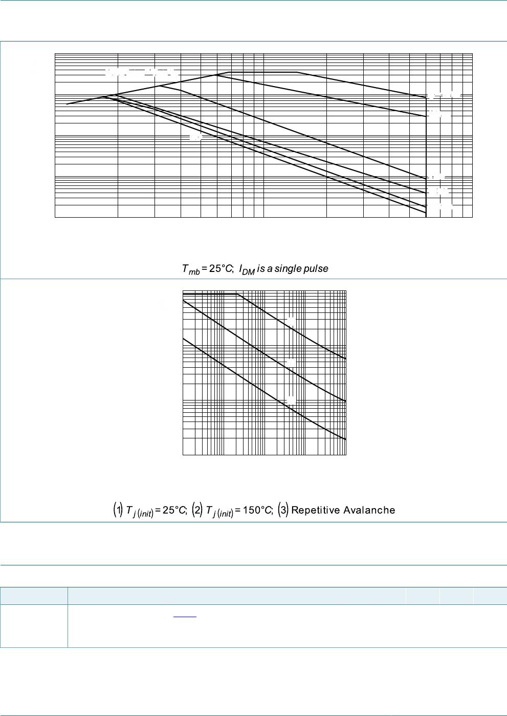
Avalanche ruggedness
E
DS(AL)S
non-repetitive drain-source
avalanche energy
I
D
= 86 A; V
sup
≤ 60 V; R
GS
= 50 Ω;
V
GS
= 5 V; T
j(init)
= 25 °C; unclamped;
Fig. 4
[1][2] - 76.5 mJ
[1] Single-pulse avalanche rating limited by maximum junction temperature of 175 °C.
[2] Refer to application note AN10273 for further information.
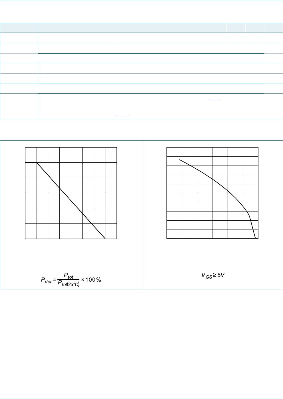
T
mb
(°C)
0 20015050 100
03aa16
40
80
120
P
der
(%)
0
Fig. 1. Normalized total power dissipation as a
function of mounting base temperature
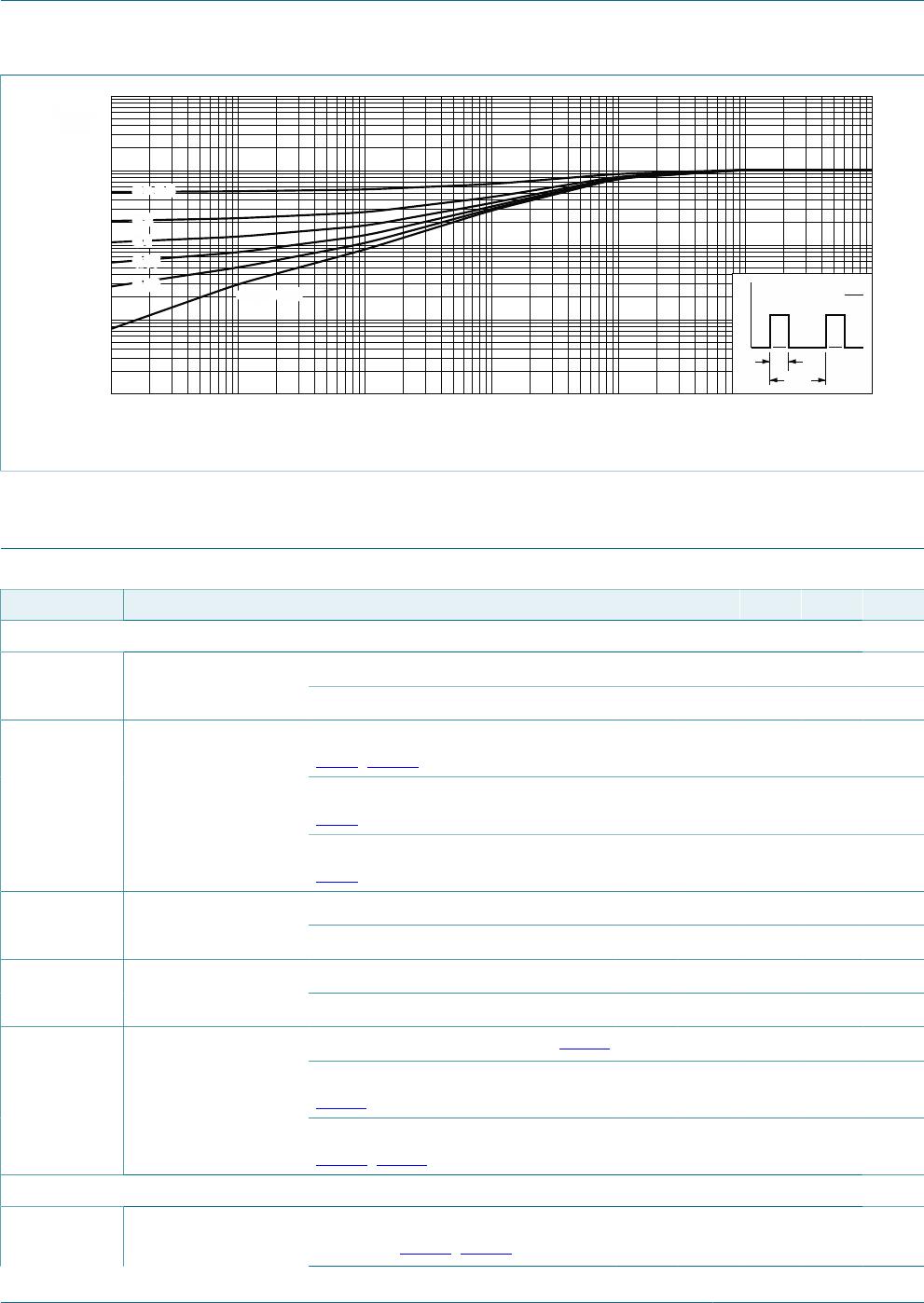
003aaj260
0 30 60 90 120 150 180
0
20
40
60
80
100
T
mb
(°C)
I
D
I
D
(A)(A)
Fig. 2. Continuous drain current as a function of
mounting base temperature