NXP Semiconductors
PSMN7R5-60YL
N-channel 60 V, 7.5 mΩ logic level MOSFET in LFPAK56
PSMN7R5-60YL All information provided in this document is subject to legal disclaimers. © NXP Semiconductors N.V. 2015. All rights reserved
Product data sheet 20 November 2015 6 / 13
Symbol Parameter Conditions Min Typ Max Unit
I
D
= 20 A; V
DS
= 48 V; V
GS
= 10 V;
T
j
= 25 °C; Fig. 13; Fig. 14
- 60.6 - nC
Q
GS
gate-source charge - 9 - nC
Q
GD
gate-drain charge
I
D
= 20 A; V
DS
= 48 V; V
GS
= 5 V;
T
j
= 25 °C; Fig. 13; Fig. 14
- 9.7 - nC
C
iss
input capacitance - 3435 4570 pF
C
oss
output capacitance - 295 355 pF
C
rss
reverse transfer
capacitance
V
GS
= 0 V; V
DS
= 25 V; f = 1 MHz;
T
j
= 25 °C; Fig. 15
- 150 205 pF
t
d(on)
turn-on delay time - 17 - ns
t
r
rise time - 30 - ns
t
d(off)
turn-off delay time - 42 - ns
t
f
fall time
V
DS
= 45 V; R
L
= 2 Ω; V
GS
= 5 V;
R
G(ext)
= 5 Ω; T
j
= 25 °C
- 26 - ns
Source-drain diode
V
SD
source-drain voltage I
S
= 20 A; V
GS
= 0 V; T
j
= 25 °C; Fig. 16 - 0.82 1.2 V
t
rr
reverse recovery time - 24 - ns
Q
r
recovered charge
I
S
= 20 A; dI
S
/dt = -100 A/µs; V
GS
= 0 V;
V
DS
= 25 V; T
j
= 25 °C
- 22.3 - nC
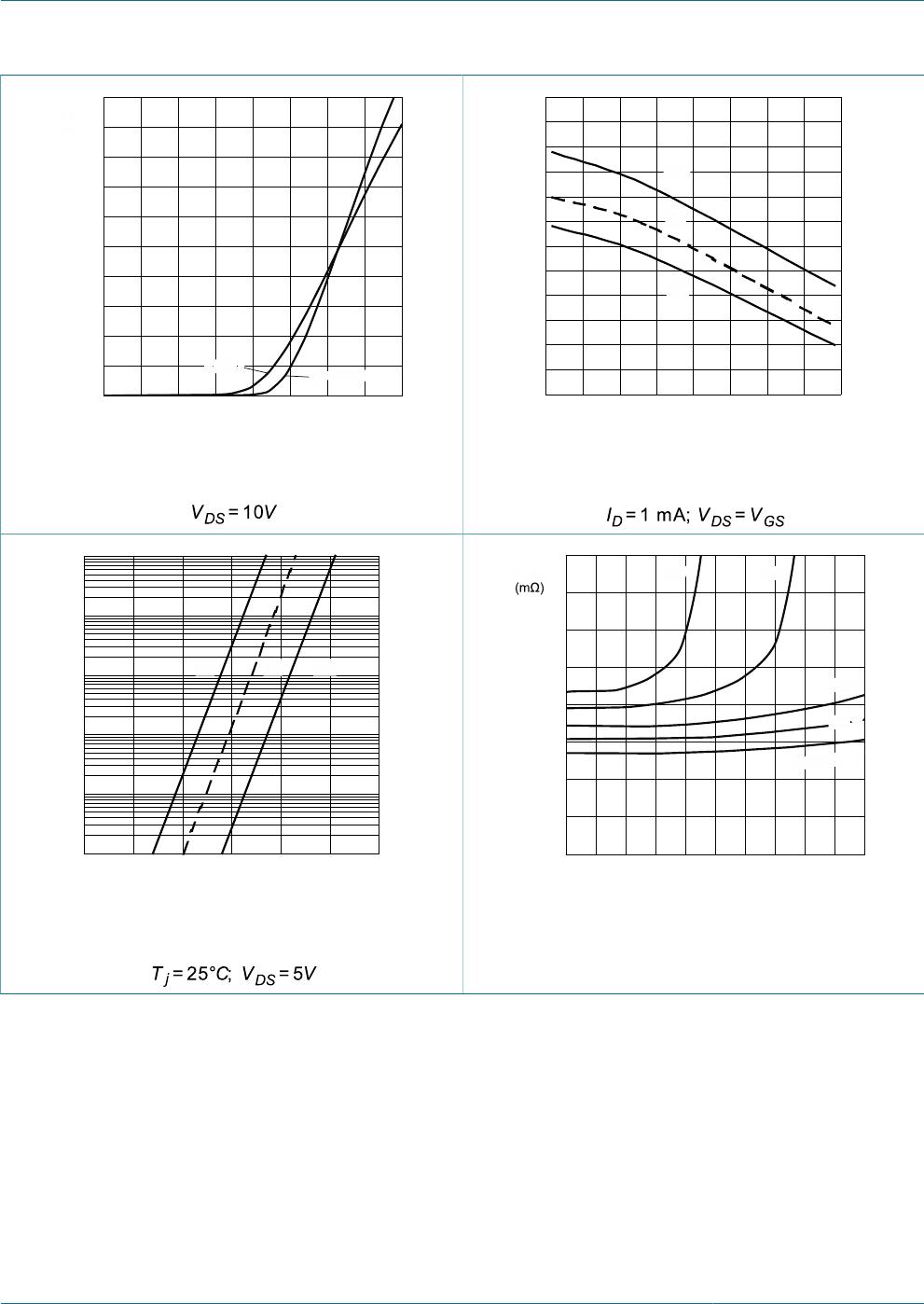
003aaj264
0 1 2 3 4
0
50
100
150
200
250
V
DS
(V)
I
D
I
D
(A)(A)
2.4 V2.4 V
2.6 V2.6 V
2.8 V2.8 V
V
GS
= 3 VV
GS
= 3 V
3.5 V3.5 V
4.5 V4.5 V
10 V10 V
T
j
= 25 °C; t
p
= 300 μs
Fig. 6. Output characteristics; drain current as a
function of drain-source voltage; typical values
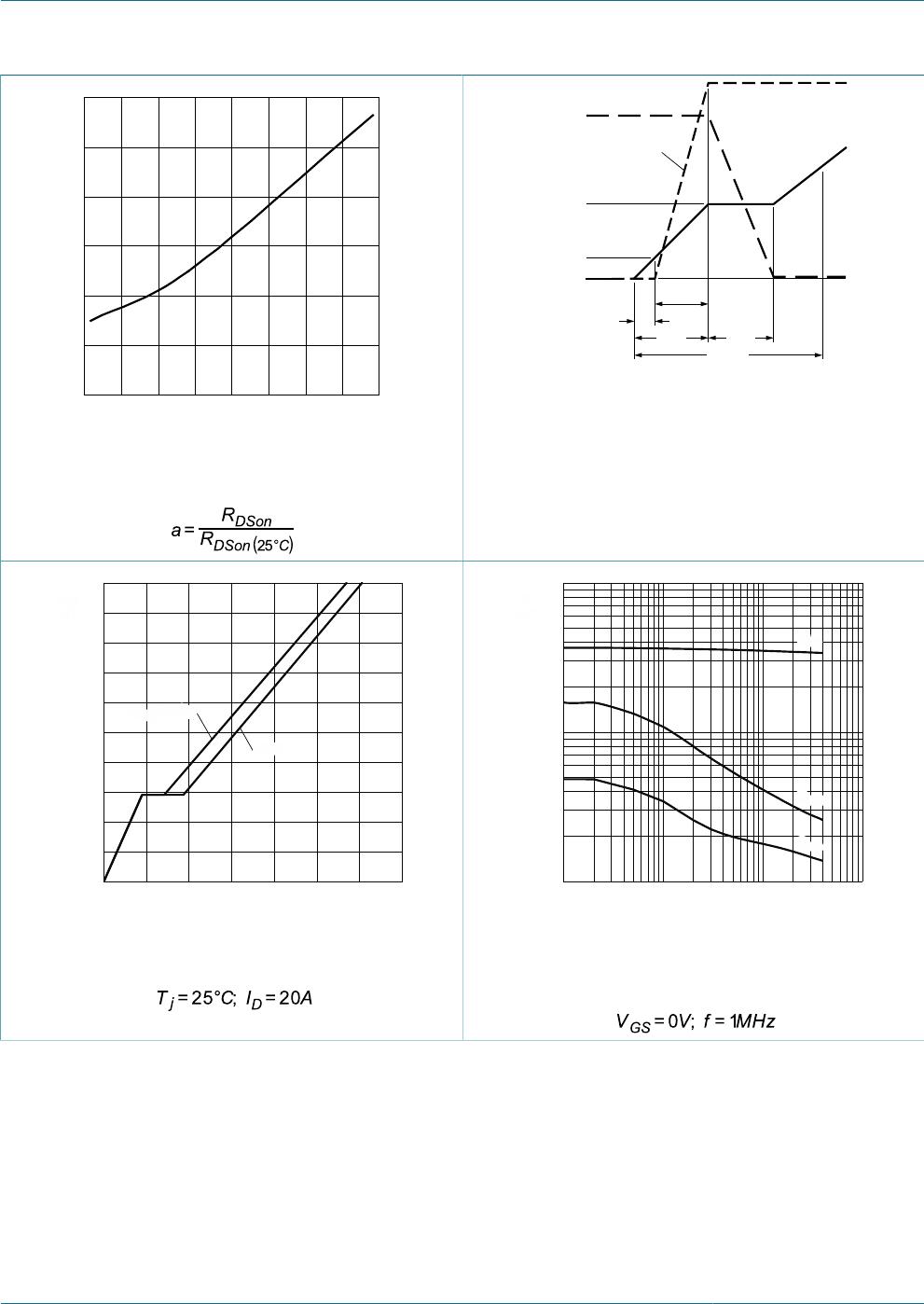
003aaj265
0 2 4 6 8 10
0
5
10
15
20
25
30
V
GS
(V)
R
DSon
R
DSon
Fig. 7. Drain-source on-state resistance as a function
of gate-source voltage; typical values