LTC1564CG#PBF

1
LTC1564
1564fa
10kHz to 150kHz
Digitally Controlled
Antialiasing Filter and 4-Bit P.G.A.
4-Bit Digitally Controlled 8th-Order Lowpass Filter
–f
CUTOFF
Adjustable from 10kHz to 150kHz in 10kHz
Steps
100dB Attenuation at 2.5 × f
CUTOFF
4-Bit Digitally Controlled Programmable Gain
Amplifier
G = 1 to 16 in 1V/V Steps
Miniature 16-Pin SSOP Package
No External Components
122dB Total System Dynamic Range
Rail-to-Rail Input and Output Range
2.7V to 10V Operation
Low Noise Mute Mode
Low Power Shutdown Mode
Available in 16-Lead Plastic SSOP Package
Antialias or Reconstruction Filtering
DSP Systems
Communications Systems
Scientific Instruments
High Resolutions (16 Bits to 20 Bits)
Processing Signals Buried in Noise
Audio Signal Processing
Programmable Data Rates
Automatic Gain Control (AGC)
Single Part Replacing Multiple Filters
Low Noise Programmable Filter with Variable Gain
The LTC
®
1564 is a new type of continuous time filter for
antialiasing, reconstruction and other band-limiting appli-
cations. No other analog components or filter expertise are
needed to use it. There is one analog input pin and one
analog output pin. The cutoff frequency (f
C
) and gain are
programmable while the shape of the lowpass response is
fixed. A latching digital interface stores f
C
and gain settings
or it can be bypassed for control directly from the pins. The
LTC1564 operates from 2.7V to 10V total (single or split
supplies) and comes in a 16-pin surface mount SSOP.
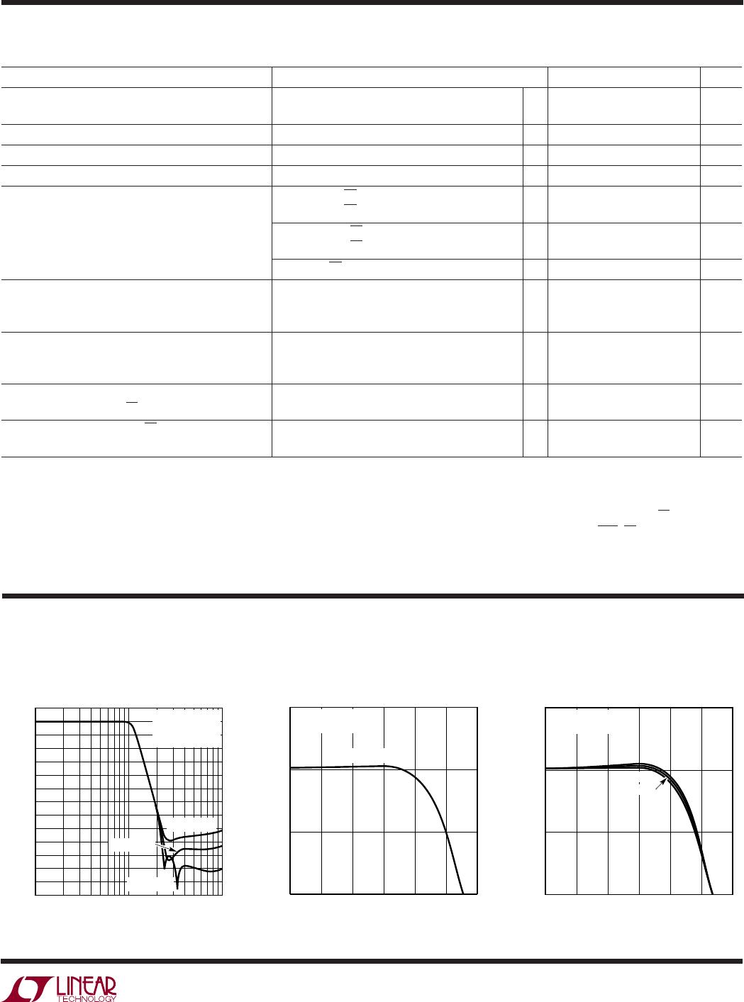
The LTC1564 is a rail-to-rail high resolution 8th-order
lowpass filter with two stopband notches, giving approxi-
mately 100dB attenuation at 2.5 times the passband cutoff
frequency f
C
(a de-facto standard for DSP front ends).
Signals with low or variable levels can be normalized with
the built-in variable gain that reduces input-referred noise
with increasing gain for a typical dynamic range (maxi-
mum signal level to minimum noise) of 122dB (20 equiva-
lent bits) with 20kHz f
C
and 118dB at 100kHz f
C
on a ±5V
supply.
Other frequency-response shapes can be provided upon
request. Please contact LTC Marketing.
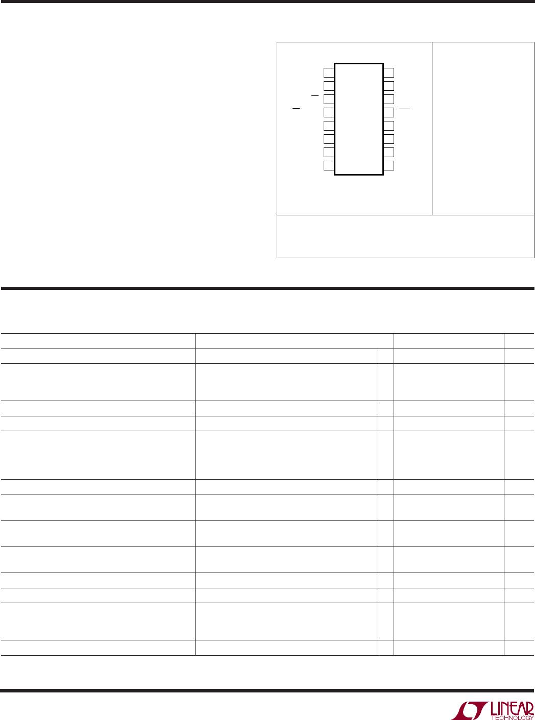
IN AGND V
+
RST G3
LTC1564
G2 G1 G0
OUT V
1234567
1564 TA01
8
16 15 14 13 12 11
GAIN CODE
FREQUENCY CODE
V
+
AND V
SUPPLIES CAN BE FROM
1.35V TO 5.25V EACH
TIE F AND G PINS TO V
+
OR V
TO
SET FREQUENCY AND GAIN
DYNAMIC RANGE 118dB TO 122dB
AT ± 5V DEPENDING ON FREQUENCY CODE
0.1µF
V
+
10 9
EN
CS/
HOLD F3 F2 F1 F0
0.1µF
ANALOG
OUT
ANALOG
IN
V
LTC1564 Programmable Range
FREQUENCY (kHz)
5
GAIN (dB)
10 100 500
1564 TA02
10
30
20
0
–10
–20
–30
–40
–50
–60
–70
–80
–120
–110
–100
–90
f
C
= 10kHz
GAIN = 1V/V
f
C
= 150kHz
GAIN = 16V/V
FEATURES
DESCRIPTIO
U
APPLICATIO S
U
TYPICAL APPLICATIO
U
, LTC and LT are registered trademarks of Linear Technology Corporation.
All other trademarks are the property of their respective owners.
2
LTC1564
1564fa
G PACKAGE
16-LEAD PLASTIC SSOP
1
2
3
4
5
6
7
8
TOP VIEW
16
15
14
13
12
11
10
9
OUT
V
EN
CS/HOLD
F3
F2
F1
F0
IN
AGND
V
+
RST
G3
G2
G1
G0
PARAMETER CONDITIONS MIN TYP MAX UNITS
Total Supply Voltage 2.7 10.5 V
Supply Current V
S
= ±1.35V, V
IN
= 0V 15 17 mA
V
S
= ±2.375V, V
IN
= 0V 16 18.5 mA
V
S
= ±5V, V
IN
= 0V 22 25 mA
Output Voltage Swing R
L
= 10k to 0V 4.5 4.65 V
P-P
Output Short-Circuit Current V
S
= ±5V ±10 mA
DC Offset Voltage Magnitude (Referred to Input) Gain = 1, 0°C to 70°C 313 mV
Gain = 1, – 40°C to 85°C
316 mV
Gain = 10, 0°C to 70°C
15 mV
Gain = 10, –40°C to 85°C
16 mV
DC AGND Reference Voltage V
S
= Single 5V Supply 2.5 V
Passband Gain f
C
= 50kHz, f
IN
= 10kHz, Gain = 1 0.1 0.3 0.8 dB
f
C
= 50kHz, f
IN
= 10KHz, Gain = 16 23.5 24.2 25.3 dB
Passband Ripple f
C
= 10kHz, 0 f
IN
9kHz (Notes 2, 3) 0.5 0.5 dB
f
C
= 150kHz, 0 f
IN
135kHz (Notes 2, 3) 0.6 1.6 dB
Roll Off at Cutoff Frequency (f
C
) (Note 3) f
C
= 10kHz (F = 0001) –1.2 0.7 0.3 dB
f
C
= 150kHz (F = 1111) –1.5 0.5 0.6 dB
Roll Off at 2f
C
(Note 3) f
C
= 10kHz –67 –63 –59 dB
Roll Off at 2.5f
C
(Note 3) f
C
= 10kHz 99 dB
Wideband Noise (Referred to Input) BW = 20kHz, f
C
= 10kHz, Gain = 1 33 µV
RMS
BW = 20kHz, f
C
= 10kHz, Gain = 16 2.5 µV
RMS
BW = 200kHz, f
C
= 100kHz, Gain = 1 50 µV
RMS
Total Harmonic Distortion f
C
= 100kHz, f
IN
= 10kHz, V
IN
= 1V
RMS
–86 dB
(Note 1)
Total Supply Voltage (V
+
to V
) .............................. 11V
Input Voltage ............................. V
+
+ 0.3V to V
– 0.3V
Output Short-Circuit Duration .......................... Indefinite
Operating Temperature Range
LTC1564C .............................................. 0°C to 70°C
LTC1564I.......................................... 40°C TO 85°C
Storage Temperature Range ................. 65°C to 150°C
Lead Temperature (Soldering, 10 sec).................. 300°C
ORDER PART
NUMBER
LTC1564CG
LTC1564IG
T
JMAX
= 125°C, θ
JA
= 130°C/ W
The
denotes specifications that apply over the full operating temperature
range, otherwise specifications are at T
A
= 25°C. V
S
= ±2.375V, f
C
= 10kHz, gain = 1, R
L
= 10k, unless otherwise noted.
ABSOLUTE AXI U RATI GS
WWWU
PACKAGE/ORDER I FOR ATIO
UU
W
ELECTRICAL CHARACTERISTICS
Consult LTC Marketing for parts specified with wider operating temperature ranges.
Order Options Tape and Reel: Add #TR
Lead Free: Add #PBF Lead Free Tape and Reel: Add #TRPBF
Lead Free Part Marking: http://www.linear.com/leadfree/
3
LTC1564
1564fa
PARAMETER CONDITIONS MIN TYP MAX UNITS
Input Impedance Gain = 1, DC V
IN
= 0V 10 k
Gain = 16, DC V
IN
= 0V 625
Output Impedance f
C
= 10kHz, f = 10kHz 30
Mute State (F = 0000) Gain F = 0000, f
IN
= 20kHz, V
IN
= 1V
RMS
–103 dB
Mute State Output Noise F = 0000, BW = 200kHz 5.4 µV
RMS
Shutdown Supply Current V
S
= ±1.35V, EN to V
+
45 75 µA
V
S
= ±1.35V, EN to V
+
150 µA
V
S
= ±2.375V, EN to V
+
100 150 µA
V
S
= ±2.375V, EN to V
+
180 µA
V
S
= ±5V, EN to V
+
(Note 4) 175 µA
Digital Input “High” Voltage V
S
= ±1.35V 1.08 V
V
S
= ±2.375V 1.90 V
V
S
= ±5V 4.50 V
Digital Input “Low” Voltage V
S
= ±1.35V –1.08 V
V
S
= ±2.375V –1.90 V
V
S
= ±5V 0.50 V
Digital Input Pull-Up or Pull-Down Current (Note 5) V
S
= ±1.35V 3.5 6 µA
(Digital Inputs Other than EN) V
S
= ±5V 13 20 µA
Digital Input Pull-Up Current (EN Input) V
S
= ±1.35V 12 µA
V
S
= ±5V 10 20 µA
The denotes specifications that apply over the full operating temperature
range, otherwise specifications are at T
A
= 25°C. V
S
= ±2.375V, f
C
= 10kHz, gain = 1, R
L
= 10k, unless otherwise noted.
ELECTRICAL CHARACTERISTICS
Note 1: Absolute Maximum Ratings are those values beyond which the life
of the device may be impaired.
Note 2: Response is tested in production at discrete frequencies f
IN
of 0.1,
0.5, 0.8 and 0.9 times f
C
.
Note 3: Relative to gain at 0.1f
C
.
Note 4: All digital inputs driven rail-to-rail. When driving digital inputs with
0V and 5V levels, the shutdown current will increase to 3.5mA (typ).
Note 5: Each digital input includes a small positive or negative current
source to float the CMOS input to V
+
or V
potential if it is unconnected.
The table shows the current due to this source when the input is driven at
the supply voltage opposite from the float potential. Pins CS/HOLD, F3, F2,
F0 and G3 to G0 float to the V
voltage, pins RST, EN and F1 to the V
+
voltage. See “Floatable Digital Inputs” in Applications Information section.
TYPICAL PERFOR A CE CHARACTERISTICS
UW
Overall Frequency Response
(Frequency Scales Normalized to f
C
)
f
IN
/f
C
–130
–70
–90
–110
10
0
–10
–30
–50
–80
–100
–120
–20
–40
–60
1564 G01
GAIN (dB)
0.1
10
1
f
C
= 10kHz
f
C
= 150kHz
f
C
= 50kHz
V
S
= SINGLE 5V
UNITY GAIN
(G CODE 0000)
FREQUENCY (kHz)
5
–10
GAIN (dB)
–5
0
5
6.25 7.5 8.75 10
1564 G02
11.25
12.5
–40°C, 25°C, 85°C
f
C
= 10kHz
SINGLE 5V SUPPLY
FREQUENCY (kHz)
50
–10
GAIN (dB)
–5
0
85°C
5
62.5 75 87.5 100
1564 G03
112.5
125
f
C
= 100kHz
SINGLE 5V SUPPLY
–40°C
25°C
Roll-Offs Over Temperature
(f
C
= 10kHz)
Roll-Offs Over Temperature
(f
C
= 100kHz)

LTC1564CG#PBF

Mfr. #:
Manufacturer:
Analog Devices Inc.
Description:
Active Filter Programmable 8th Order Filter and PGA
Lifecycle:
New from this manufacturer.
Delivery:
DHL FedEx Ups TNT EMS
Payment:
T/T Paypal Visa MoneyGram Western Union