10
LTC1564
1564fa
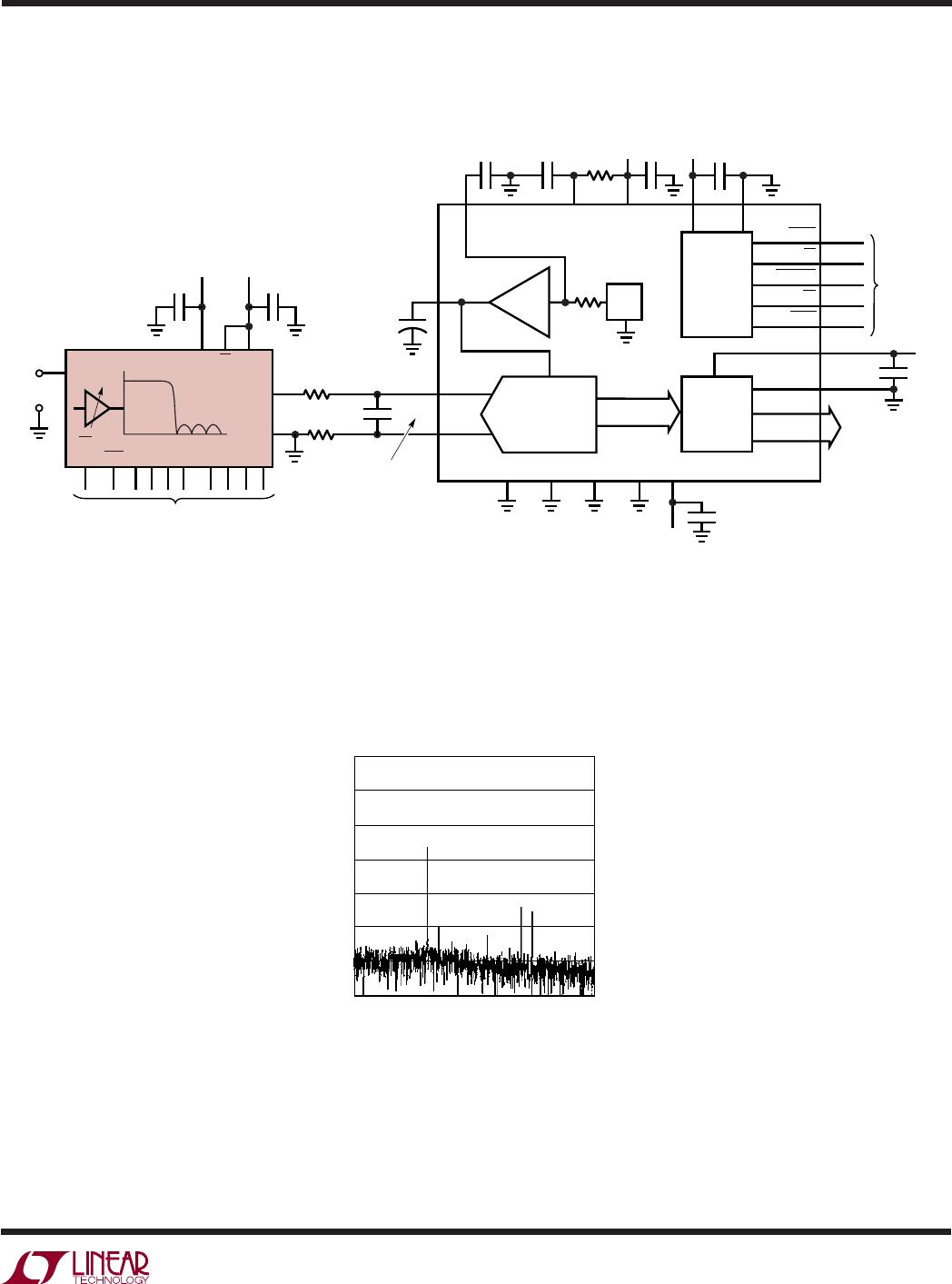
APPLICATIO S I FOR ATIO
WUUU
levels that program the part for enabled F and G pins
(CS/HOLD = 0), 20kHz f
C
and unity passband gain. There-
fore six connections (power pins, EN to logic 0, AGND, IN
and OUT) are enough to set up a working 20kHz lowpass
filter, and additional pins can be connected as necessary
to select different f
C
or gain.
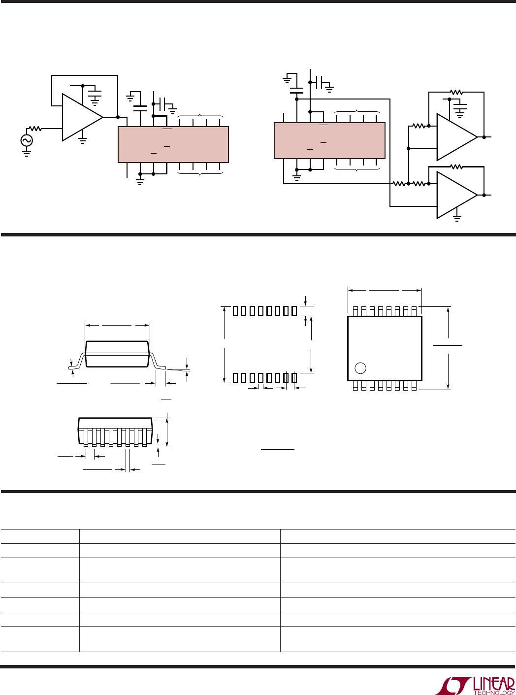
This feature of floatable logic inputs is intended for rapid
prototyping and experimentation. Floating the logic inputs
is not recommended for production designs because,
depending on construction details, the high impedances
of these inputs may permit unwanted interference cou-
pling and consequent erroneous digital inputs to the
LTC1564.
Also, it may be necessary to consider the effect of the pull-
up and pull-down current sources on the logic that drives
the LTC1564. In particular, if the LTC1564 operates from
±5V but receives digital inputs from logic using 5V and 0V,
CMOS logic levels will be compatible but the possibility
exists of the LTC1564 pulling current out of the driving logic
at those LTC1564 inputs that are capable of floating to logic
0. That is because the small current sources at these in-
puts return to V
–
, not to 0V. If the driving logic presents a
high impedance or three-state output, the LTC1564’s in-
put current may pull this output below 0V, although the
current is limited to about 10µA. The system designer
should be aware of this possibility and ensure that any such
current flow is compatible with the driving logic.
Mute State
The Mute mode keeps the filter powered as in normal
filtering but “turns off” the signal path for minimal signal
transmission (approximately –100dB) and reduced out-
put noise. This feature may be useful for gating a signal
source on and off, or for system calibration procedures.
Note however that the DC output in the Mute state may
shift by some millivolts compared to normal filtering
because the internal signal path changes. Recovery from
Mute, like other transient responses in a filter, proceeds at
the time scale of the filter’s pole-zero time constants and
therefore is faster at the higher f
C
settings (that is, at the
higher F codes).
The LTC1564 enters the Mute state when the F bits at the
latch output (Figure 3) become 0000. (It can be remem-
bered as a “zero-bandwidth” frequency setting.) This is
achieved either by presenting a 0000 code to the F inputs
and lowering the CS/HOLD input to enable the latch, or
alternatively at any time by lowering RST, which immedi-
ately resets the latch contents to all zeroes. Such a reset
also occurs normally at the application of power, unless
CS/HOLD is low and a nonzero pattern at the F inputs
overrides the brief power-on reset. In the Mute state, the
G gain-control inputs have no effect.
Output noise in Mute is largely thermal and wideband
(unlike in normal filtering, where the filter’s response
affects the noise spectrum). Typical Mute-state output
noise is 5.4µV
RMS
in 200kHz measurement bandwidth
and less than 3µV
RMS
in 40kHz bandwidth. It has occa-
sionally happened elsewhere in the electronics industry
that someone would characterize a circuit or system by
comparing its output level in normal operation to the noise
level in a Mute state as though this were a normal signal-
to-noise ratio (SNR), which it is not, because this signal
and noise exist only at different times. A scrupulous name
for such a measure is SMR, signal-to-mute ratio. Accord-
ingly in a 40kHz bandwidth, the LTC1564 can exhibit an
SMR exceeding 120dB.
Construction and Instrumentation Cautions
Electrically clean construction is important in applications
seeking the full dynamic range or high stopband rejection
of the LTC1564. Short, direct wiring will minimize parasitic
capacitance and inductance. High quality supply bypass
capacitors of 0.1µF near the chip provide good decoupling
from a clean, low inductance power source. But several
inches of wire (i.e., a few microhenrys of inductance) from
the power supplies, unless decoupled by substantial ca-
pacitance (≥ 10µF) near the chip, can cause a high-Q LC
resonance in the hundreds of kHz in the chip’s supplies or
ground reference. This may impair stopband rejection and
other specifications at those frequencies. In stringent filter
applications we have often found that a compact, carefully
laid out printed circuit board with good ground plane
makes a difference in both stopband rejection and distor-
tion. Finally, equipment to measure filter performance can
itself introduce distortion or noise floors. Checking for
these limits with a wire replacing the filter is a prudent
routine procedure.