LTC1564CG#PBF

4
LTC1564
1564fa
TYPICAL PERFOR A CE CHARACTERISTICS
UW
Detail of Stopband Response
Passband Gain, Phase
and Group Delay
f
C
(kHz)
10
GAIN (dB)
0.50
0.25
0
70 110
1564 G04
0.75
–1.00
30 50
90 130 150
–1.25
–1.50
V
S
= SINGLE 5V
T
A
= 25°C
FREQUENCY (kHz)
15
GAIN (dB)
–80
–60
–40
55
1564 G05
–100
–120
–90
–70
–50
–110
–130
–140
25
35
45
65
f
C
= 10kHz
V
S
= ±5V
T
A
= 25°C
FREQUENCY (kHz)
2
GAIN (dB)
PHASE (DEGREES)
–15
–5
5
10
1546 G06
–25
–35
–20
–10
0
–30
–40
–45
270
–90
90
450
630
360
–180
0
540
–720
810
DELAY (µs)
300
400
500
200
100
250
350
450
150
50
0
4
6
8
12
GAIN
f
C
= 10kHz
PHASE
GROUP DELAY
Passband Roll-Off at f
IN
= f
C
vs f
C
2V/DIV
1564 G07
200µs/DIV
OUTPUT
f
C
= 10kHz
UNITY GAIN
V
S
= ±5V
INPUT
100µs/DIV
1564 G08
INPUT, 1V/DIV (PULSE WIDTH 10µs)
OUTPUT, 100mV/DIV
f
C
= 10kHz
UNITY GAIN
V
S
= ± 5V
Rectangular Pulse Response Short-Pulse Response
Triangular-Wave Time Response SNR vs Input Voltage
THD + Noise vs Input Voltage
(f
C
= 10kHz)
200µs/DIV
5V/DIV
1564 G09
f
C
= 10kHz
f
IN
= 1kHz
UNITY GAIN
V
S
= ± 5V
INPUT
OUTPUT
INPUT VOLTAGE (V
P-P
)
–80
(THD + NOISE)/SIGNAL (dB)
–60
–50
–30
–20
0.001 0.1 1 10
1564 G11
–100
0.01
–40
–70
–90
3V SUPPLY
5V SUPPLY
±5V SUPPLY
f
C
= 10kHz
f
IN
= 1kHz
INPUT VOLTAGE (V
P-P
)
30
10
SIGNAL/NOISE (dB)
50
70
90
110
0.001 0.1 1 10
1564 G10
0
0.01
140
130
20
40
60
80
100
120
GAIN = 16
f
C
= 20kHz
GAIN = 1
f
C
= 100kHz
GAIN = 1
f
C
= 20kHz
GAIN = 16
f
C
= 100kHz
LIMIT FOR 5V TOTAL SUPPLY
LIMIT FOR 10V TOTAL SUPPLY
PASSBAND INPUT
(f
IN
< f
C
)
5
LTC1564
1564fa
TYPICAL PERFOR A CE CHARACTERISTICS
UW
UU
U
PI FU CTIO S
OUT (Pin 1): Analog Output. In normal filtering, this is the
output of an internal operational amplifier and is capable
of swinging essentially to any voltage between the power
supply rails (that is, between V
+
and V
). This output is
designed to drive a nominal load of 5k and 50pF. For
lowest signal distortion it should be loaded as lightly as
possible. The output can drive lower resistances than 5k,
but distortion may increase, and the output current will
limit at approximately ±10mA. Capacitances higher than
50pF should be isolated by a series resistor of 500 to
preserve AC stability. In the Mute state (F code 0000 or
RST = 0), the output operates as in normal filtering but the
gain from the IN pin becomes zero and the output noise is
reduced. In the shutdown state (EN = 1 or EN open
circuited), most of the circuitry in the LTC1564 shuts off
and the OUT pin assumes a high impedance state.
V
, V
+
(Pins 2, 14): Power Supply Pins. The V
+
and V
pins should be bypassed with 0.1µF capacitors to an
adequate analog ground plane using the shortest possible
wiring. Electrically clean supplies and a low impedance
ground are important for the high dynamic range and high
stopband suppression available from the LTC1564 (see
further details under AGND). Low noise linear power
supplies are recommended. Switching supplies are not
recommended because of the inevitable risk of their
switching noise coupling into the signal path, reducing
dynamic range.
EN (Pin 3): CMOS-Level Digital Chip Enable Input. Logic 1
or open circuiting this pin causes a shutdown mode with
reduced supply current. The active circuitry in the LTC1564
shuts off and its output assumes a high impedance state.
If F and G bits are latched (CS/HOLD = 1) during the
shutdown state, the latch will retain its contents.
A small pull-up current source at the EN input causes the
LTC1564 to be in shutdown state if the EN pin is left open.
Therefore, the user must connect the EN pin to logic 0 (V
or optionally 0V with ±5V supplies) for normal filter
operation.
CS/HOLD (Pin 4): CMOS-Level Digital Enable Input for the
Latch Holding F and G Bits. Logic 0 makes the latch
transparent so that the F and G inputs directly control the
filter’s cutoff frequency and gain. Logic 1 holds the last
values of these inputs prior to the transition. This pin floats
to logic 0 (V
) when open circuited because of a small
current source (see Electrical Characteristics, Note 5).
F3, F2, F1, F0 (Pins 5, 6, 7, 8): CMOS-Level Digital
Frequency Control (“F Code”) Inputs. F3 is the most
significant bit (MSB). These pins program the LTC1564’s
cutoff frequency f
C
through the internal latch, which
THD + Noise vs Input Voltage
(f
C
= 100kHz)
INPUT VOLTAGE (V
P-P
)
–80
(THD + NOISE)/SIGNAL (dB)
–60
–50
–30
–20
0.001 0.1 1 10
1564 G12
–100
0.01
–40
–70
–90
3V SUPPLY
5V SUPPLY
±5V SUPPLY
f
C
= 100kHz
f
IN
= 10kHz
BASEBAND GAIN SETTING
2
1
10
100
4
8
1564 G13
INPUT-REFERRED NOISE (µV
RMS
)
1
16
f
C
= 100kHz
f
C
= 10kHz
FREQUENCY (Hz)
–60
GAIN (dB)
–40
–30
–10
10
0.1k 10k 100k 1M
1564 G14
–80
1k
–20
–50
–70
0
f
C
= 10kHz
V
S
= ±2.5V
NEGATIVE SUPPLY
V
+
SUPPLY BYPASS = 0.1µF
V
SUPPLY BYPASS = NONE
POSITIVE SUPPLY
V
+
SUPPLY BYPASS = NONE
V
SUPPLY BYPASS = 0.1µF
Noise vs Frequency
and Gain Settings
Power Supply Rejection
vs Frequency
6
LTC1564
1564fa
UU
U
PI FU CTIO S
passes the bits directly when the CS/HOLD input is at logic
0. When CS/HOLD changes to logic 1, the F pins cease to
have effect and the latch holds the previous values. The F
code controls the filter’s cutoff frequency f
C
in 10kHz steps
up to 150kHz, as summarized in Table 1.
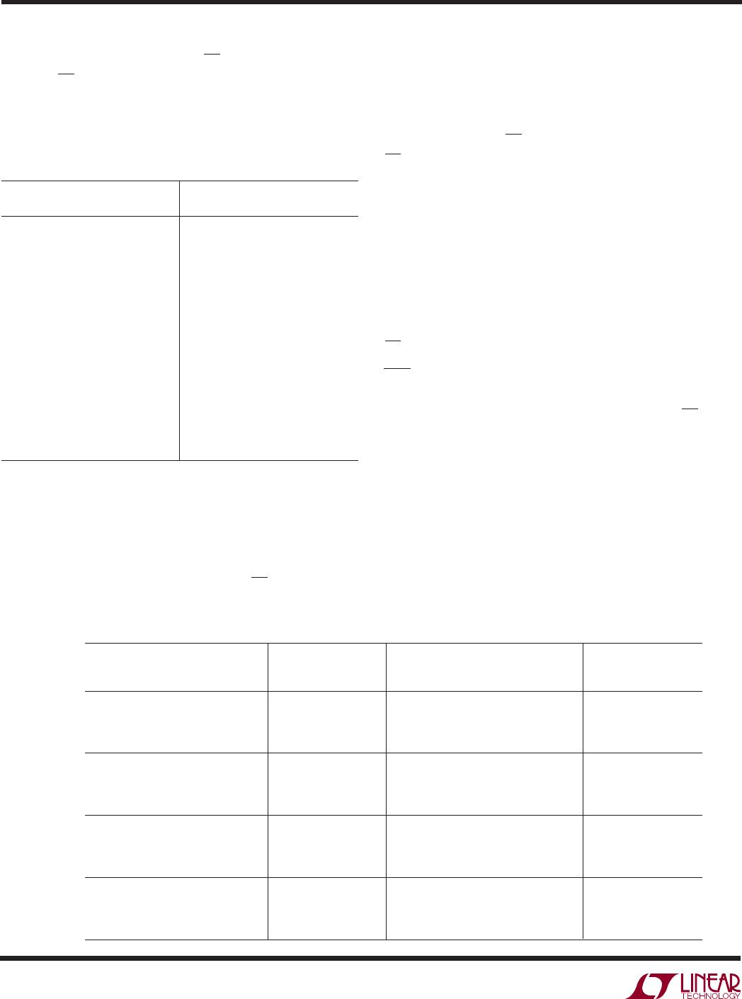
Table 1
F3 F2 F1 F0 NOMINAL F
C
(AT OUTPUT OF INTERNAL LATCH) (CUTOFF FREQUENCY)
0000 0 (Mute State: Filter Gain is Zero)
0001 10kHz
0010 20kHz
0011 30kHz
0100 40kHz
0101 50kHz
0110 60kHz
0111 70kHz
1000 80kHz
1001 90kHz
1010 100kHz
1011 110kHz
1100 120kHz
1101 130kHz
1110 140kHz
1111 150kHz
Thus f
C
is proportional to the binary value of the F code.
Note that small current sources pull F1 to V
+
and F3, F2
and F0 to V
when these pins are left unconnected (see
Electrical Characteristics, Note 5). This sets an F code
input of 0010 (2, in decimal form) by default, giving an f
C
of 20kHz in normal filtering operation, if CS/HOLD is logic
0 or is open circuited.
G0, G1, G2, G3 (Pins 9, 10, 11, 12): CMOS-Level Digital
Gain Control (“G Code”) Inputs. G3 is the most significant
bit (MSB). These pins program the LTC1564’s passband
gain through the internal latch, which passes the bits
directly when the CS/HOLD input is at logic 0. When
CS/HOLD changes to logic 1, the G pins cease to have
effect and the latch retains the previous input values. This
gain control is linear in amplitude: nominal passband gain
of the LTC1564 is the binary value of the G code, plus one
as shown in Table 2.
Note that small current sources pull the G pins to V
when
these pins are left unconnected (see Electrical Character-
istics, Note 5). This sets a G code input of 0000 by default,
giving unity passband gain in normal filtering operation, if
CS/HOLD is logic 0 or is open circuited.
RST (Pin 13): CMOS-Level Asynchronous Reset Input.
Logic 0 on this pin immediately resets the internal F and G
latch to all zeros, regardless of the state of the CS/HOLD
pin or the F or G input pins. This causes the LTC1564 to
enter a mute state (powered but with zero signal gain)
because of the resulting F = 0000 command. Logic 1
permits the other pins to control F and G. This pin floats to
logic 1 (V
+
) when open circuited because of a small
current source (see Electrical Characteristics, Note 5). A
brief internal reset (shorter than the analog settling time of
the filter) also occurs when power is first applied.
NOMINAL NOMINAL
G3 G2 G1 G0 PASSBAND GAIN (VOLTS PEAK-TO-PEAK) INPUT IMPEDANCE
(VOLT/VOLT) (dB) DUAL 5V SINGLE 5V SINGLE 3V (k)
0000 1 0 10 5.0 3.0 10
0001 2 6.0 5 2.5 1.5 5
0010 3 9.5 3.33 1.67 1.0 3.33
0011 4 12 2.5 1.25 0.75 2.5
0100 5 14.0 2 1 0.6 2
0101 6 15.6 1.67 0.83 0.5 1.67
0110 7 16.9 1.43 0.71 0.43 1.43
0111 8 18.1 1.25 0.63 0.38 1.25
1000 9 19.1 1.1 0.56 0.33 1.11
1001 1020.0 1.0 0.50 0.30 1
1010 1120.8 0.91 0.45 0.27 0.91
1011 1221.6 0.83 0.42 0.25 0.83
1100 1322.3 0.77 0.38 0.23 0.77
1101 1422.9 0.71 0.36 0.21 0.71
1110 1523.5 0.67 0.33 0.20 0.66
1111 1624.1 0.63 0.31 0.19 0.63
(AT OUTPUT OF INTERNAL LATCH)
MAXIMUM INPUT SIGNAL LEVEL
Table 2

LTC1564CG#PBF

Mfr. #:
Manufacturer:
Analog Devices Inc.
Description:
Active Filter Programmable 8th Order Filter and PGA
Lifecycle:
New from this manufacturer.
Delivery:
DHL FedEx Ups TNT EMS
Payment:
T/T Paypal Visa MoneyGram Western Union