LTC2941
13
2941fb
For more information www.linear.com/LTC2941
applicaTions inFormaTion
Alert Response Protocol
In a system where several slaves share a common interrupt
line, the master can use the alert response address (ARA)
to determine which device initiated the interrupt (Figure 9).
FROM MASTER TO SLAVE
S W
ADDRESS REGISTER DATA
FROM SLAVE TO MASTER
2941 F05
A: ACKNOWLEDGE (LOW)
A: NOT-ACKNOWLEDGE (HIGH)
R: READ BIT (HIGH)
W: WRITE BIT (LOW)
S: START CONDITION
P: STOP CONDITION
A A A
0
1100100 01h FCh
0 0 0
P
Figure 5. Writing FCh to LTC2941 Control Register (B)
S W
ADDRESS REGISTER DATA
2941 F06
A A A
0
1100100 02h F0h 01h
0 0 0
0
P
DATA
A
Figure 6. Writing F001h to the LTC2941 Accumulated Charge Registers (C, D)
S W
ADDRESS REGISTER S
2941 F07
A A ADDRESS
0
1100100 00h 1
0 0 1100100
0
P
R
1
A
81h
DATA
A
Figure 7. Reading the LTC2941 Status Register (A)
S W
ADDRESS REGISTER S
2941 F08
A A ADDRESS
0
1100100 02h 1
0 0 1100100
0
P
R
0
A
80h
DATA
01h
DATA
A
1
A
Figure 8. Reading the LTC2941 Accumulated Charge Registers (C, D)
S R
ALERT RESPONSE ADDRESS DEVICE ADDRESS
2941 F09
A
1
0001100 11001001
0 1
P
A
Figure 9. LTC2941 Serial Bus SDA Alert Response Protocol
The master initiates the ARA procedure with a START con-
dition and the special 7-bit ARA bus address (0001100)
followed by the read bit
(R) = 1. If the LTC2941 is asserting
the AL/CC pin in alert mode, it acknowledges and responds
by sending its 7-bit bus address (1100100) and a 1. While
LTC2941
14
2941fb
For more information www.linear.com/LTC2941
applicaTions inFormaTion
it is sending its address, it monitors the SDA pin to see
if another device is sending an address at the same time
using standard I
2
C bus arbitration. If the LTC2941 is send-
ing a 1 and reads a 0 on the SDA pin on the rising edge of
SCL, it assumes another device with a lower address is
sending and the LTC2941 immediately aborts its transfer
and waits for the next ARA cycle to tr
y again. If transfer
is successfully completed, the LTC2941 will stop pulling
down the AL/CC pin and will not respond to further ARA
requests until a new alert event occurs.
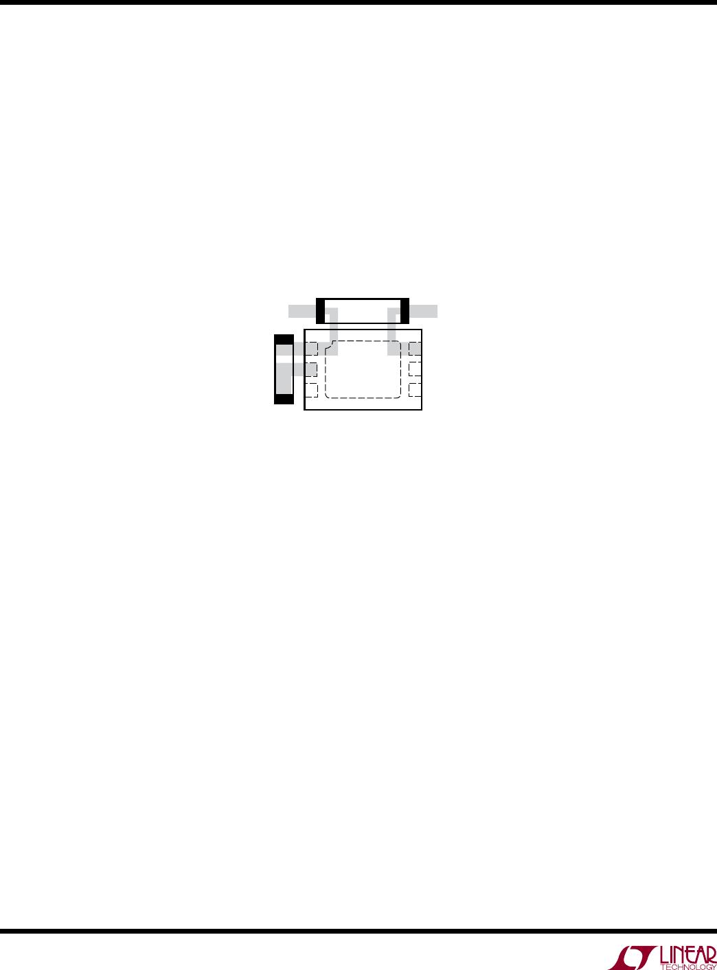
PC Board Layout Recommendations
Keep all traces as short as possible to minimize noise and
inaccuracy. Use a 4-wire Kelvin sense connection for the
sense resistor, locating the LTC2941 close to the resis
-
tor with short sense traces to SENSE
+
and SENSE
. Use
wider traces from the resistor to the battery, load and/or
charger (see Figure 10). Put the bypass capacitor close
to SENSE
+
and GND.
LTC2941
2941 F10
R
SENSE
TO BATTERY
TO
CHARGER/LOAD
4
5
6
3
2
C
1
Figure 10. Kelvin Connection on Sense Resistor
LTC2941
15
2941fb
For more information www.linear.com/LTC2941
package DescripTion
3.00 ±0.10
(2 SIDES)
2.00 ±0.10
(2 SIDES)
NOTE:
1. DRAWING TO BE MADE A JEDEC PACKAGE OUTLINE M0-229 VARIATION OF (TBD)
2. DRAWING NOT TO SCALE
3. ALL DIMENSIONS ARE IN MILLIMETERS
4. DIMENSIONS OF EXPOSED PAD ON BOTTOM OF PACKAGE DO NOT INCLUDE
MOLD FLASH. MOLD FLASH, IF PRESENT, SHALL NOT EXCEED 0.15mm ON ANY SIDE
5. EXPOSED PAD SHALL BE SOLDER PLATED
6. SHADED AREA IS ONLY A REFERENCE FOR PIN 1 LOCATION ON THE
TOP AND BOTTOM OF PACKAGE
0.40 ± 0.10
BOTTOM VIEW—EXPOSED PAD
1.65 ± 0.10
(2 SIDES)
0.75 ±0.05
R = 0.115
TYP
R = 0.05
TYP
1.35 ±0.10
(2 SIDES)
1
3
64
PIN 1 BAR
TOP MARK
(SEE NOTE 6)
0.200 REF
0.00 – 0.05
(DCB6) DFN 0405
0.25 ± 0.05
0.50 BSC
PIN 1 NOTCH
R0.20 OR 0.25
× 45° CHAMFER
0.25 ± 0.05
1.35 ±0.05
(2 SIDES)
RECOMMENDED SOLDER PAD PITCH AND DIMENSIONS
1.65 ±0.05
(2 SIDES)
2.15 ±0.05
0.70 ±0.05
3.55 ±0.05
PACKAGE
OUTLINE
0.50 BSC
DCB Package
6-Lead Plastic DFN (2mm × 3mm)
(Reference LTC DWG # 05-08-1715 Rev A)
Please refer to http://www.linear.com/designtools/packaging/ for the most recent package drawings.

LTC2941IDCB#TRMPBF

Mfr. #:
Manufacturer:
Analog Devices / Linear Technology
Description:
Battery Management Bat Gas Gauge w/ I2C Int
Lifecycle:
New from this manufacturer.
Delivery:
DHL FedEx Ups TNT EMS
Payment:
T/T Paypal Visa MoneyGram Western Union