ADUM3210TRZ-EP

ADuM3210-EP/ADuM3211-EP Enhanced Product
Rev. A | Page 10 of 12
PIN CONFIGURATIONS AND FUNCTION DESCRIPTIONS
V
DD1
1
V
IA
2
V
IB
3
G
ND
1
4
V
DD2
8
V
OA
7
V
OB
6
GND
2
5
ADuM3210-EP
TOP VIEW
(Not to Scale)
13094-003
Figure 4. ADuM3210-EP Pin Configuration
V
DD1
1
V
OA
2
V
IB
3
G
ND
1
4
V
DD2
8
V
IA
7
V
OB
6
GND
2
5
ADuM3211-EP
TOP VIEW
(Not to Scale)
13094-016
Figure 5. ADuM3211-EP Pin Configuration
Table 20. ADuM3210-EP Pin Function Descriptions
Pin No. Mnemonic Description
1 V
DD1
Supply Voltage for Isolator Side 1,
3.0 V to 5.5 V.
2 V
IA
Logic Input A.
3 V
IB
Logic Input B.
4 GND
1
Ground 1. Ground reference for
Isolator Side 1.
5 GND
2
Ground 2. Ground reference for
Isolator Side 2.
6 V
OB
Logic Output B.
7 V
OA
Logic Output A.
8 V
DD2
Supply Voltage for Isolator Side 2,
3.0 V to 5.5 V.
Table 21. ADuM3211-EP Pin Function Descriptions
Pin No. Mnemonic Description
1 V
DD1
Supply Voltage for Isolator Side 1,
3.0 V to 5.5 V.
2 V
OA
Logic Output A.
3 V
IB
Logic Input B.
4 GND
1
Ground 1. Ground reference for
Isolator Side 1.
5 GND
2
Ground 2. Ground reference for
Isolator Side 2.
6 V
OB
Logic Output B.
7 V
IA
Logic Input A.
8 V
DD2
Supply Voltage for Isolator Side 2,
3.0 V to 5.5 V.
TRUTH TABLES
Table 22. ADuM3210-EP Truth Table (Positive Logic)
V
IA
Input
1
V
IB
Input
1
V
DD1
State V
DD2
State V
OA
Output
1
V
OB
Output
1
Notes
H H Powered Powered H H
L L Powered Powered L L
H L Powered Powered H L
L H Powered Powered L H
X X Unpowered Powered L L
Outputs return to the input state within
1 μs of V
DDI
power restoration
X X Powered Unpowered Indeterminate Indeterminate
Outputs return to the input state within
1 μs of V
DDO
power restoration
1
H is logic high, L is logic low, and X is don’t care.
Table 23. ADuM3211-EP Truth Table (Positive Logic)
V
IA
Input
1
V
IB
Input
1
V
DD1
State V
DD2
State V
OA
Output
1
V
OB
Output
1
Notes
H H Powered Powered H H
L L Powered Powered L L
H L Powered Powered H L
L H Powered Powered L H
X X Unpowered Powered Indeterminate L
Outputs return to the input state within
1 μs of V
DDI
power restoration
X X Powered Unpowered L Indeterminate
Outputs return to the input state within
1 μs of V
DDO
power restoration
1
H is logic high, L is logic low, and X is don’t care.
Enhanced Product ADuM3210-EP/ADuM3211-EP
Rev. A | Page 11 of 12
TYPICAL PERFORMANCE CHARACTERISTICS
DATA RATE (Mbps)
CURRENT/CHANNEL (mA)
0
0
6
2
8
10
10
20 30
5.0V
3.3V
4
13094-004
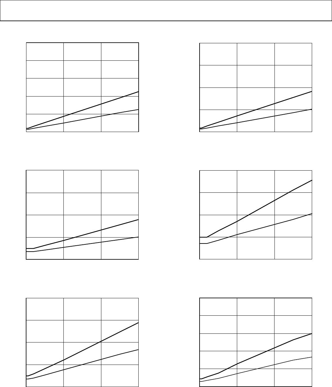
Figure 6. Typical Input Supply Current per Channel vs. Data Rate
for 5.0 V and 3.3 V Operation
DATA RATE (Mbps)
CURRENT/CHANNEL (mA)
0
0
3
2
1
4
10 20 30
5.0V
3.3V
13094-005
Figure 7. Typical Output Supply Current per Channel vs. Data Rate
for 5.0 V and 3.3 V Operation (No Output Load)
DATA RATE (Mbps)
CURRENT/CHANNEL (mA)
0
0
3
2
1
4
10 20 30
5.0V
3.3V
13094-006
Figure 8. Typical Output Supply Current per Channel vs. Data Rate
for 5.0 V and 3.3 V Operation (15 pF Output Load)
DATA RATE (Mbps)
CURRENT (mA)
0
0
15
10
5
20
10 20 30
13094-007
5.0V
3.3V
Figure 9. ADuM3210-EP Typical I
DD1
Supply Current vs. Data Rate
for 5.0 V and 3.3 V Operation
DATA RATE (Mbps)
CURRENT (mA)
0
0
3
2
1
4
10 20
30
5.0V
3.3V
13094-008
Figure 10. ADuM3210-EP Typical I
DD2
Supply Current vs. Data Rate
for 5.0 V and 3.3 V Operation
DATA RATE (Mbps)
CURRENT (mA)
0
0
6
2
8
10
10
20 30
5.0V
3.3V
4
13094-015
Figure 11. ADuM3211-EP Typical I
DD1
or I
DD2
Supply Current vs. Data Rate
for 5.0 V and 3.3 V Operation
ADuM3210-EP/ADuM3211-EP Enhanced Product
Rev. A | Page 12 of 12
OUTLINE DIMENSIONS
CONTROLLING DIMENSIONS ARE IN MILLIMETERS; INCH DIMENSIONS
(IN PARENTHESES) ARE ROUNDED-OFF MILLIMETER EQUIVALENTS FOR
REFERENCE ONLY AND ARE NOT APPROPRIATE FOR USE IN DESIGN.
COMPLIANT TO JEDEC STANDARDS MS-012-AA
012407-A
0.25 (0.0098)
0.17 (0.0067)
1.27 (0.0500)
0.40 (0.0157)
0.50 (0.0196)
0.25 (0.0099)
45°
1.75 (0.0688)
1.35 (0.0532)
SEATING
PLANE
0.25 (0.0098)
0.10 (0.0040)
4
1
8 5
5.00 (0.1968)
4.80 (0.1890)
4.00 (0.1574)
3.80 (0.1497)
1.27 (0.0500)
BSC
6.20 (0.2441)
5.80 (0.2284)
0.51 (0.0201)
0.31 (0.0122)
COPLANARITY
0.10
Figure 12. 8-Lead Standard Small Outline Package [SOIC_N]
Narrow Body
(R-8)
Dimensions shown in millimeters and (inches)
ORDERING GUIDE
Model
1
Number
of Inputs,
V
DD1
Side
Number
of Inputs,
V
DD2
Side
Maximum
Data Rate
(Mbps)
Maximum
Propagation
Delay, 5 V (ns)
Maximum
Pulse Width
Distortion (ns)
Temperature
Range
Package
Description
Package
Option
2
ADuM3210TRZ-EP 2 0 25 50 3 −55°C to +125°C 8-Lead SOIC_N R-8
ADuM3210TRZ-EP-RL7 2 0 25 50 3 −55°C to +125°C 8-Lead SOIC_N R-8
ADuM3211TRZ-EP 1 1 25 50 4 −55°C to +125°C 8-Lead SOIC_N R-8
ADuM3211TRZ-EP-RL7 1 1 25 50 4 −55°C to +125°C 8-Lead SOIC_N R-8
1
Z = RoHS Compliant Part.
2
R-8 means 8-lead, narrow body SOIC_N.
©2015 Analog Devices, Inc. All rights reserved. Trademarks and
registered trademarks are the property of their respective owners.
D13094-0-10/15(A)

ADUM3210TRZ-EP

Mfr. #:
Manufacturer:
Analog Devices Inc.
Description:
Digital Isolators DUAL-CHANNEL DIGITAL ISOLATORS
Lifecycle:
New from this manufacturer.
Delivery:
DHL FedEx Ups TNT EMS
Payment:
T/T Paypal Visa MoneyGram Western Union