MAX6952
4-Wire Interfaced, 2.7V to 5.5V,
4-Digit 5
7 Matrix LED Display Driver
4 _______________________________________________________________________________________
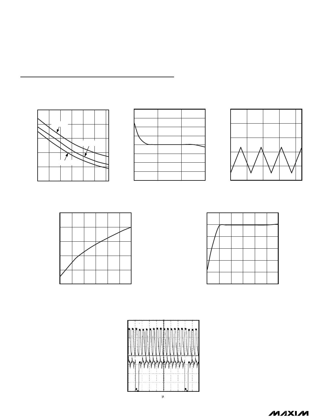
Typical Operating Characteristics
(Typical application circuit, V+ = 3.3V, LED forward voltage = 2.4V, scan limit set to 4 digits, T
A
= +25°C, unless otherwise noted.)
3.80
3.90
4.10
4.00
4.20
4.30
-40 0-20 20
40
60 80
INTERNAL OSCILLATOR
FREQUENCY vs. TEMPERATURE
MAX6952 toc01
TEMPERATURE (°C)
OSCILLATOR FREQUENCY (MHz)
V+ = 3.3V
V+ = 2.7V
V+ = 5V
INTERNAL OSCILLATOR FREQUENCY
vs. SUPPLY VOLTAGE
MAX6952 toc02
SUPPLY VOLTAGE (V)
OSCILLATOR FREQUENCY (MHz)
4.53.5
3.7
3.8
3.9
4.0
4.1
4.2
4.3
4.4
3.6
2.5 5.5
0
0.5
1.5
1.0
2.0
2.5
0
400
200
600
800
INTERNAL OSCILLATOR
WAVEFORM AT OSC
MAX6952 toc03
TIMELINE (ns)
VOLTAGE AT OSC (V)
80
85
95
90
100
105
2.5 3.53.0 4.0 4.5 5.0 5.5
DEAD CLOCK OSCILLATOR FREQUENCY
vs. SUPPLY VOLTAGE
MAX6952 toc04
SUPPLY VOLTAGE (V)
OSCILLATOR FREQUENCY (kHz)
0.95
0.97
0.96
0.99
0.98
1.00
1.01
2.5 3.5 4.03.0 4.5 5.0 5.5
SEGMENT SOURCE CURRENT
vs. SUPPLY VOLTAGE
MAX6952 toc05
SUPPLY VOLTAGE (V)
CURRENT NORMALIZED TO 40mA
WAVEFORMS AT O2 (PIN 3) AND O14
(PIN 28) 15/16 INTENSITY
GROUND FOR
ANODE
(PIN O14)
MAX6952 toc06
GROUND FOR
CATHODE
(PIN O3) 220 s/div
Detailed Description
The MAX6952 is a serially interfaced display driver that
can drive four digits of 5
7 cathode-row dot-matrix
displays. The MAX6952 can drive either four monocolor
digits (Table 1) or two bicolor digits (Table 2). The
MAX6952 includes a 128-character font map compris-
ing 104 predefined characters and 24 user-definable
characters. The predefined characters follow the Arial
font, with the addition of the following common sym-
bols: £, , ¥, °, µ, ±, , and . The 24 user-definable
characters are uploaded by the user into on-chip RAM
through the serial interface and are lost when the
device is powered down. Figure 1 is the MAX6952
functional diagram.
Serial Interface
The MAX6952 communicates through an SPI-compati-
ble 4-wire serial interface. The interface has three
inputs, clock (CLK), chip select (CS), and data in (DIN),
and one output, data out (DOUT). CS must be low to
clock data into or out of the device, and DIN must be
stable when sampled on the rising edge of CLK. DOUT
is stable on the rising edge of CLK. Note that while the
SPI protocol expects DOUT to be high impedance
when the MAX6952 is not being accessed, DOUT on
the MAX6952 is never high impedance.
MAX6952
4-Wire Interfaced, 2.7V to 5.5V,
4-Digit 5
7 Matrix LED Display Driver
_______________________________________________________________________________________ 5
Pin Description
PIN
SSOP PDIP
NAME FUNCTION
1, 2, 3, 614, 23, 24 1, 2, 3, 715, 26, 27 O0 to O13
LED Cathode Drivers. O0 to O13 outputs sink current from
the displays cathode rows.
4, 5, 16 4, 5, 6, 18 GND Ground
15 17 ISET
Segment Current Setting. Connect ISET to GND through
series resistor R
SET
to set the peak current.
17 19 BLINK Blink Clock Output. Output is open drain.
18 20 DIN
Serial Data Input. Data is loaded into the internal 16-bit shift
register on the rising edge of the CLK.
19 21 CLK
Serial-Clock Input. On the rising edge of CLK, data is
shifted into the internal shift register. On the falling edge of
CLK, data is clocked out of DOUT. CLK input is active only
while CS is low.
20 22 DOUT
Serial Data Output. Data clocked into DIN is output to
DOUT 15.5 clock cycles later. Data is clocked out on the
rising edge of CLK. Output is push-pull.
21 23 CS
Chip-Select Input. Serial data is loaded into the shift register
while CS is low. The last 16 bits of serial data are latched on
CSs rising edge.
22 24 OSC
Multiplex Clock Input. To use the internal oscillator, connect
capacitor C
SET
from OSC to GND. To use the external
clock, drive OSC with a 1MHz to 8MHz CMOS clock.
2531, 34, 35, 36 2834, 38, 39, 40 O14 to O23
LED Anode Drivers. O14 to O23 outputs source current to
the displays anode columns.
32, 33 35, 36, 37 V+
Positive Supply Voltage. Bypass V+ to GND with a 47µF
bulk capacitor and a 0.1µF ceramic capacitor.
MAX6952
CLK and DIN may be used to transmit data to other
peripherals. The MAX6952 ignores all activity on CLK
and DIN except when CS is low.
Control and Operation Using the 4-Wire Interface
Controlling the MAX6952 requires sending a 16-bit
word. The first byte, D15 through D8, is the command
byte (Table 3), and the second byte, D7 through D0, is
the data byte.
Connecting Multiple MAX6952s to the 4-Wire Bus
Multiple MAX6952s may be daisy-chained by connect-
ing the DOUT of one device to the DIN of the next, and
driving CLK and CS lines in parallel (Figure 6). Data at
DIN propagates through the internal shift registers and
appears at DOUT 15.5 clock cycles later, clocked out
on the falling edge of CLK. When sending commands
to daisy-chained MAX6952s, all devices are accessed
at the same time. An access requires (16 x n) clock
cycles, where n is the number of MAX6952s connected
together. To update just one device in a daisy-chain,
the user can send the no-op command (0x00) to the
others.
Writing Device Registers
The MAX6952 contains a 16-bit shift register into which
DIN data are clocked on the rising edge of SCLK, when
CS is low. When CS is high, transitions on SCLK have
no effect. When CS goes high, the 16 bits in the shift
4-Wire Interfaced, 2.7V to 5.5V,
4-Digit 5
7 Matrix LED Display Driver
6 _______________________________________________________________________________________
DIGIT O0 O1 O2 O3 O4 O5 O6 O7 O8 O9 O10 O11 O12 O13 O14 O15 O16 O17 O18 O19 O20 O21 O22 O23
1
Digit 0 rows (cathodes) R1 to R7
Digit 1 rows (cathodes) R1 to R7
Digit 0 columns (anodes)
C1 to C5
Digit 1 columns
(anodes) C6 to C10
2
Digit 2 rows (cathodes) R1 to R7
Digit 3 rows (cathodes) R1 to R7
Digit 2 columns (anodes)
C1 to C5
Digit 3 columns
(anodes) C6 to C10
Table 1. Connection Scheme for Four Monocolor Digits
DIGIT O0 O1 O2 O3 O4 O5 O6 O7 O8 O9 O10 O11 O12 O13 O14 O15 O16 O17 O18 O19 O20 O21 O22 O23
Digit 0 columns (anodes) C1 to C10
1 Digit 0 rows (cathodes) R1 to R14
- the 5 green anodes - - the 5 red anodes -
Digit 1 columns (anodes) C1 to C10
2 Digit 1 rows (cathodes) R1 to R14
- the 5 green anodes - - the 5 red anodes -
Table 2. Connection Scheme for Two Bicolor Digits
D15 D14 D13 D12 D11 D10 D9 D8 D7 D6 D5 D4 D3 D2 D1 D0
R/W ADDRESS MSB DATA LSB
Table 3. Serial-Data Format (16 Bits)
ISET
OSC
BLINK
CLK
CS
DIN
DOUT
SERIAL INTERFACE
RAM
BLINK
SPEED
SELECT
CONFIGURATION
REGISTERS
CHARACTER
GENERATOR
ROM
CHARACTER
GENERATOR
RAM
CURRENT
SOURCE
DIVIDER/
COUNTER
NETWORK
ROW
MULTIPLEXER
PWM
BRIGHTNESS
CONTROL
LED
DRIVERS
O0 TO O23
MAX6952
Figure 1. Functional Diagram

MAX6952EAX+

Mfr. #:
Manufacturer:
Maxim Integrated
Description:
LED Display Drivers 2.7-5.5V 4-Digit 5x7 Matrix LED Driver
Lifecycle:
New from this manufacturer.
Delivery:
DHL FedEx Ups TNT EMS
Payment:
T/T Paypal Visa MoneyGram Western Union

Products related to this Datasheet