AD5320
Rev. C | Page 15 of 20
APPLICATIONS
USING REF19X AS A POWER SUPPLY FOR AD5320
Because the supply current required by the AD5320 is
extremely low, an alternative option is to use a REF19x voltage
reference (REF195 for 5 V or REF193 for 3 V) to supply the
required voltage to the part (see
Figure 32). This is especially
useful if the power supply is noisy or if the system supply
voltages are at some value other than 5 V or 3 V (such as 15 V).
The REF19x outputs a steady supply voltage for the AD5320. If
the low dropout REF195 is used, the current it needs to supply
to the AD5320 is 140 μA. This is with no load on the output of
the DAC. When the DAC output is loaded, the REF195 also
needs to supply the current to the load. The total current
required (with a 5 kΩ load on the DAC output) is:
140 μA + (5 V/5 kΩ) = 1.14 mA
The load regulation of the REF195 is typically 2 ppm/mA,
which results in an error of 2.3 ppm (11.5 μV) for the 1.14 mA
current drawn from it. This corresponds to a 0.009 LSB error.
REF195
AD5320
DIN
SCLK
SYNC
15
V
5V
140µA
V
OUT
= 0V TO 5V
3-WIRE
SERIAL
INTERFACE
00934-032
Figure 32. REF195 as Power Supply to AD5320
BIPOLAR OPERATION USING THE AD5320
The AD5320 is designed for single-supply operation but a bipolar
output range is also possible using the circuit in
Figure 33. The
circuit below gives an output voltage range of ±5 V. Rail-to-rail
operation at the amplifier output is achievable using an AD820 or
an OP295 as the output amplifier.
The output voltage for any input code can be calculated as
follows:
×
+
×
×=
1
2
1
21
4096 R
R
V
R
RR
D
VV
DDDD
O
where
D represents the input code in decimal (0 to 4095).
With
V
DD
= 5 V, R1 = R2 = 10 kΩ:
V
D
V
O
5
4096
10
×
=
This is an output voltage range of ±5 V with 000 hex
corresponding to a −5 V output and FFF hex corresponding to
a +5 V output.
3-WIRE SERIAL INTERFACE
+5V
AD5320
10µF
0.1µF
V
DD
V
OUT
R1 = 10k
R2 = 10k
+5V
±5
V
–5V
AD820/
OP295
00934-033
Figure 33. Bipolar Operation with the AD5320
USING AD5320 WITH AN OPTO-ISOLATED
INTERFACE
For process control applications in industrial environments, it is
often necessary to use an opto-isolated interface to protect and
isolate the controlling circuitry from any hazardous common-
mode voltages that can occur in the area where the DAC is
functioning. Opto-isolators provide isolation in excess of 3 kV.
Because the AD5320 uses a 3-wire serial logic interface, it
requires only three opto-isolators to provide the required
isolation (see
Figure 34). The power supply to the part also
needs to be isolated. This is done by using a transformer. On the
DAC side of the transformer, a 5 V regulator provides the 5 V
supply required for the AD5320.
V
DD
0.1µF
V
DD
10k
10k
V
DD
10k
5V
REGULATOR
V
OUT
GND
DIN
SYNC
SCLK
POWER
10µF
V
DD
SYNC
SCLK
DATA
AD5320
00934-034
Figure 34. AD5320 with An Opto-Isolated Interface
AD5320
Rev. C | Page 16 of 20
POWER SUPPLY BYPASSING AND GROUNDING
When accuracy is important in a circuit, it is helpful to consider
carefully the power supply and ground return layout on the
board. The printed circuit board containing the AD5320 should
have separate analog and digital sections, each having its own
area of the board. If the AD5320 is in a system where other
devices require an AGND to DGND connection, the connec-
tion should be made at one point only. This ground point
should be as close as possible to the AD5320.
The power supply to the AD5320 should be bypassed with 10 μF
capacitors and 0.1 μF capacitors. The capacitors should be physi-
cally as close as possible to the device with the 0.1 μF capacitors
ideally against the device. The 10 μF capacitors are the tantalum
bead type. It is important that the 0.1 μF capacitors have low
effective series resistance (ESR) and effective series inductance
(ESI), such as common ceramic types of capacitors. The 0.1 μF
capacitors provide a low impedance path to ground for high
frequencies caused by transient currents due to internal logic
switching.
The power supply line itself should have as large a trace as
possible to provide a low impedance path and reduce glitch
effects on the supply line. Clocks and other fast switching
digital signals should be shielded from other parts of the board
by digital ground. Avoid crossover of digital and analog signals
if possible. When traces cross on opposite sides of the board,
ensure that they run at right angles to each other to reduce
feedthrough effects through the board. The best board layout
technique is the microstrip technique where the component
side of the board is dedicated to the ground plane only and the
signal traces are placed on the solder side. However, this is not
always possible with a two-layer board.
AD5320
Rev. C | Page 17 of 20
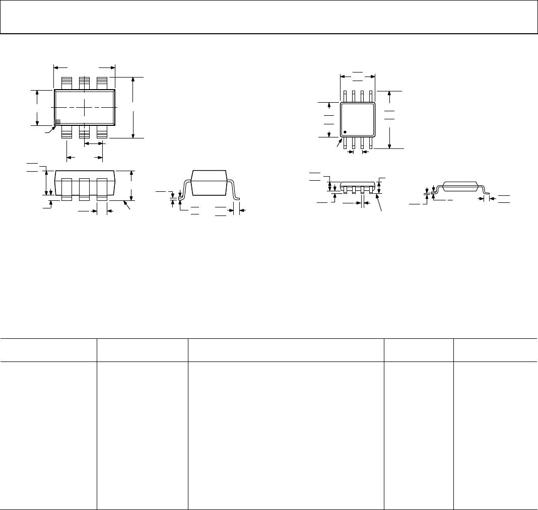
OUTLINE DIMENSIONS
1 3
45
2
6
2.90 BSC
1.60 BSC
2.80 BSC
1.90
BSC
0.95 BSC
0.22
0.08
10°
0.50
0.30
0.15 MAX
1.30
1.15
0.90
SEATING
PLANE
1.45 MAX
0.60
0.45
0.30
PIN 1
INDICATOR
COMPLIANT TO JEDEC STANDARDS MO-178-AB
Figure 35. 6-Lead Small Outline Transistor Package [SOT-23]
(RT-6)
Dimensions shown in millimeters
COMPLIANT TO JEDEC STANDARDS MO-187-AA
0.80
0.60
0.40
4
8
1
5
PIN 1
0.65 BSC
SEATING
PLANE
0.38
0.22
1.10 MAX
3.20
3.00
2.80
COPLANARITY
0.10
0.23
0.08
3.20
3.00
2.80
5.15
4.90
4.65
0.15
0.00
0.95
0.85
0.75
Figure 36. 8-Lead Mini Small Outline Package [MSOP]
(RM-8)
Dimensions shown in millimeters
ORDERING GUIDE
Model
Temperature Range
Package Description
Branding
Package Option
AD5320BRM −40°C to +105°C 8-Lead Mini Small Outline Package [MSOP] D4B RM-8
AD5320BRM-REEL −40°C to +105°C 8-Lead Mini Small Outline Package [MSOP] D4B RM-8
AD5320BRM-REEL7 −40°C to +105°C 8-Lead Mini Small Outline Package [MSOP] D4B RM-8
AD5320BRMZ
1
−40°C to +105°C 8-Lead Mini Small Outline Package [MSOP] D9N RM-8
AD5320BRMZ-REEL
1
−40°C to +105°C 8-Lead Mini Small Outline Package [MSOP] D9N RM-8
AD5320BRMZ-REEL7
1
−40°C to +105°C 8-Lead Mini Small Outline Package [MSOP] D9N RM-8
AD5320BRT-500RL7 −40°C to +105°C 6-Lead Small Outline Transistor Package [SOT-23] D4B RT-6
AD5320BRT-REEL −40°C to +105°C 6-Lead Small Outline Transistor Package [SOT-23] D4B RT-6
AD5320BRT-REEL7 −40°C to +105°C 6-Lead Small Outline Transistor Package [SOT-23] D4B RT-6
AD5320BRTZ-500RL7
1
−40°C to +105°C 6-Lead Small Outline Transistor Package [SOT-23] D9N RT-6
AD5320BRTZ-REEL
1
−40°C to +105°C 6-Lead Small Outline Transistor Package [SOT-23] D9N RT-6
AD5320BRTZ-REEL7
1
−40°C to +105°C 6-Lead Small Outline Transistor Package [SOT-23] D9N RT-6
1
Z = Pb-free part.

AD5320BRTZ-500RL7

Mfr. #:
Manufacturer:
Analog Devices Inc.
Description:
Digital to Analog Converters - DAC 12 Bit Vout 8uS
Lifecycle:
New from this manufacturer.
Delivery:
DHL FedEx Ups TNT EMS
Payment:
T/T Paypal Visa MoneyGram Western Union