LTC4007
10
4007fc
OPERATION
keep a low forward voltage drop from drain to source. If the
voltage between DCIN and CLN drops to less than 25mV,
the input FET is turned off slowly. If the voltage between
DCIN and CLN is ever less than –25mV, then the input FET
is turned off in less than 10μs to prevent signifi cant reverse
current from fl owing in the input FET. In this condition, the
ACP pin is driven low and the charger is disabled.
Battery Charger Controller
The LTC4007 charger controller uses a constant off-time,
current mode step-down architecture. During normal
operation, the top MOSFET is turned on each cycle when
the oscillator sets the SR latch and turned off when the
main current comparator I
CMP
resets the SR latch. While
the top MOSFET is off, the bottom MOSFET is turned
on until either the inductor current trips the current
comparator I
REV
or the beginning of the next cycle. The
oscillator uses the equation:
t
VV
Vf
OFF
DCIN BAT
DCIN OSC
=
to set the bottom MOSFET on time. The result is a nearly
constant switching frequency over a wide input/output
voltage range. This activity is diagrammed in Figure 1.
Table 1. Truth Table For Indicator States
MODE DCIN SHDN ACP** LOBAT FLAG** FAULT** I
CL
TIMER
STATE CHG**
Shut down by low adapter voltage <BAT LOW LOW LOW HIGH HIGH LOW Reset HIGH
Charging a low bat >BAT LOW HIGH LOW HIGH* HIGH* HIGH* Running LOW
Normal charging >BAT LOW HIGH HIGH HIGH HIGH* HIGH* Running LOW
Input current limited charging >BAT LOW HIGH HIGH HIGH* HIGH* LOW Running LOW
Charger paused due to thermistor out of range >BAT LOW HIGH X X LOW
(from
NTC)
HIGH Paused LOW
Shut down by SHDN pin X HIGH X X HIGH HIGH LOW Reset HIGH
Terminated by low-battery fault (Note 1) >BAT LOW HIGH LOW HIGH* LOW LOW >T/4 HIGH
(Faulted)
Timer is reset when FLAG goes low, then
terminates after 1/4 T
>BAT LOW HIGH HIGH LOW HIGH LOW >T/4
after
FLAG =
LOW
HIGH
(Waiting for
Restart
Terminated by expired timer >BAT LOW HIGH HIGH HIGH HIGH LOW >T HIGH
(Waiting for
Restart
Charge termination defeated X X X X X X X X Forced LOW
Shut down by undervoltage lockout >BAT +
<UVL
LOW HIGH HIGH HIGH HIGH* LOW Reset HIGH*
*Most probable condition X = Don’t care, ** Open-drain output HIGH = OPEN with pull-up
Note 1: If a depleted battery is inserted while the charger is in this state,
the charger must be reset to initiate charging.
TGATE
OFF
ON
BGATE
INDUCTOR
CURRENT
t
OFF
TRIP POINT SET BY ITH VOLTAGE
ON
OFF
4006 F01
Figure 1
LTC4007
11
4007fc
OPERATION
The peak inductor current, at which I
CMP
resets the SR
latch, is controlled by the voltage on ITH. ITH is in turn
controlled by several loops, depending upon the situation
at hand. The average current control loop converts the
voltage between CSP and BAT to a representative cur-
rent. Error amp CA2 compares this current against the
desired current programmed by RPROG at the PROG pin
and adjusts ITH until:
V
R
VV Ak
k
REF
PROG
CSP BAT
=
Ω
–..
.
11 67 3 01
301
μ
therefore,
I
V
R
A
k
CHARGE MAX
REF
PROG
()
–.
.
=
Ω
11 67
301
μ
RR
SENSE
The voltage at BAT is divided down by an internal resis-
tor divider and is used by error amp EA to decrease ITH
if the divider voltage is above the 1.19V reference. When
the charging current begins to decrease, the voltage at
PROG will decrease in direct proportion. The voltage at
PROG is then given by:
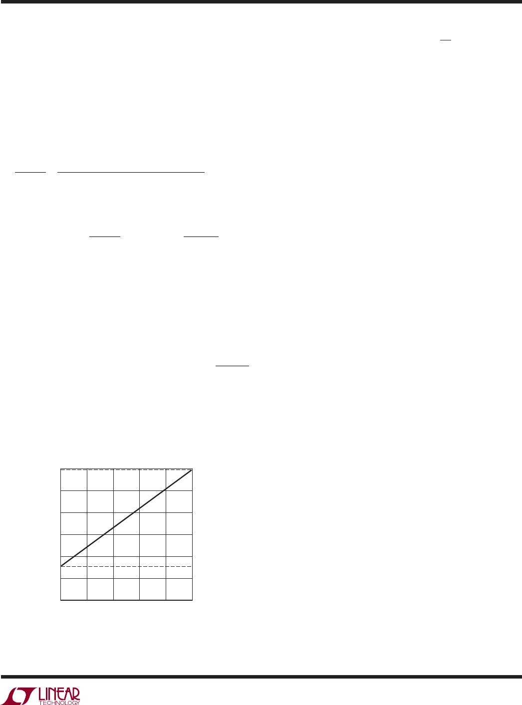
VI R Ak
R
PROG CHARGE SENSE
PROG
=+Ω
()
•..11 67 3 01μ
3301.kΩ
V
PROG
is plotted in Figure 2.
The amplifi er CL1 monitors and limits the input current,
normally from the AC adapter to a preset level (100mV/R
CL
).
At input current limit, CL1 will decrease the ITH voltage,
I
CHARGE
(% OF MAXIMUM CURRENT)
0
0
V
PROG
(V)
0.2
0.4
0.6
0.8
20 40
60 80
100
4007 F02
1.0
1.2 1.19V
0.309V
Figure 2. V
PROG
vs I
CHARGE
thereby reducing charging current. The I
CL
indicator output
will go low when this condition is detected and the FLAG
indicator will be inhibited if it is not already LOW.
If the charging current decreases below 10% to 15%
of programmed current while engaged in input current
limiting, BGATE will be forced low to prevent the charger
from discharging the battery. Audible noise can occur in
this mode of operation.
An overvoltage comparator guards against voltage tran-
sient overshoots (>7% of programmed value). In this
case, both MOSFETs are turned off until the overvoltage
condition is cleared. This feature is useful for batteries
which “load dump” themselves by opening their protection
switch to perform functions such as calibration or pulse
mode charging.
PWM Watchdog Timer
There is a watchdog timer that observes the activity on
the BGATE and TGATE pins. If TGATE stops switching for
more than 40μs, the watchdog activates and turns off the
top MOSFET for about 400ns. The watchdog engages to
prevent very low frequency operation in dropout—a po-
tential source of audible noise when using ceramic input
and output capacitors.
Charger Start-Up
When the charger is enabled, it will not begin switching
until the ITH voltage exceeds a threshold that assures initial
current will be positive. This threshold is 5% to 15% of the
maximum programmed current. After the charger begins
switching, the various loops will control the current at a
level that is higher or lower than the initial current. The
duration of this transient condition depends upon the loop
compensation, but is typically less than 100μs.
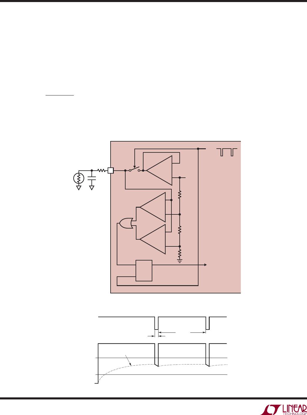
Thermistor Detection
The thermistor detection circuit is shown in Figure 3. It
requires an external resistor and capacitor in order to
function properly.
The thermistor detector performs a sample-and-hold
function. An internal clock, whose frequency is determined
LTC4007
12
4007fc
OPERATION
by the timing resistor connected to R
T
, keeps switch S1
closed to sample the thermistor:
t
SAMPLE
= 127.5 • 20 • R
RT
• 17.5pF = 13.8ms,
for R
RT
= 309k
The external RC network is driven to approximately 4.5V
and settles to a fi nal value across the thermistor of:
V
VR
RR
RTH FINAL
TH
TH
()
.•
=
+
45
9
This voltage is stored by C7. Then the switch is opened
for a short period of time to read the voltage across the
thermistor.
t
HOLD
= 10 • R
RT
• 17.5pF = 54μs,
for R
RT
= 309k
When the t
HOLD
interval ends the result of the thermistor
testing is stored in the D fl ip-fl op (DFF). If the voltage at
NTC is within the limits provided by the resistor divider
feeding the comparators, then the NOR gate output will
be low and the DFF will set T
BAD
to zero and charging will
continue. If the voltage at NTC is outside of the resistor
divider limits, then the DFF will set T
BAD
to one, the charger
will be shut down, FAULT pin is set low and the timer will
be suspended until T
BAD
returns to zero (see Figure 4).
9
R9
32.4k
C7
0.47μF
R
TH
10k
NTC
+
+
+
NTC
LTC4007
S1
60k
~4.5V
CLK
45k
15k
TBAD
4007 F03
D
C
Q
CLK
(NOT TO
SCALE)
V
NTC
t
SAMPLE
VOLTAGE ACROSS THERMISTOR
t
HOLD
4007 F04
COMPARATOR HIGH LIMIT
COMPARATOR LOW LIMIT
Figure 3
Figure 4

LTC4007EGN#PBF

Mfr. #:
Manufacturer:
Analog Devices / Linear Technology
Description:
Battery Management 4A, Li-Ion Charger w/ Termination
Lifecycle:
New from this manufacturer.
Delivery:
DHL FedEx Ups TNT EMS
Payment:
T/T Paypal Visa MoneyGram Western Union

Products related to this Datasheet