LTC4007
9
4007fc
TEST CIRCUIT
–
+
–
+
EA
LT1055
LTC4007
V
REF
CHEM
3C4C
BAT
DIVIDER/
MUX
16
7
15
CSP
14
ITH
0.6V
4007 TC
10
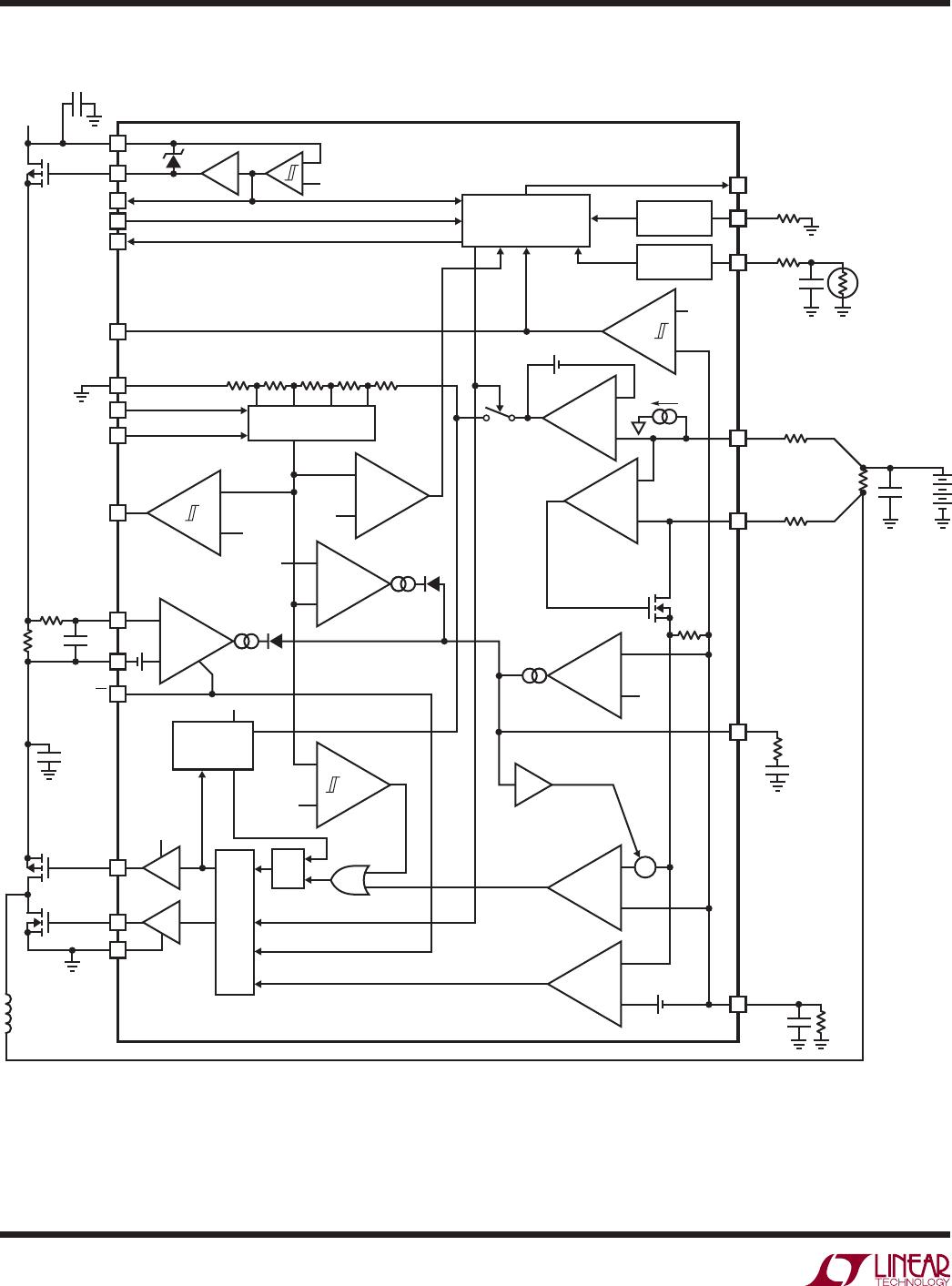
OPERATION
Overview
The LTC4007 is a synchronous current mode PWM step-
down (buck) switcher battery charger controller. The charge
current is programmed by the combination of a program
resistor (R
PROG
) from the PROG pin to ground and a sense
resistor (R
SENSE
) between the CSP and BAT pins. The fi nal
fl oat voltage is programmed to one of four values (12.3V,
12.6V, 16.4V, 16.8V) with ±1% maximum accuracy using
pins 3C4C and CHEM. Charging begins when the potential
at the DCIN pin rises above the voltage at BAT (and the
UVLO voltage) and the SHDN pin is low; the CHG pin is
set low. At the beginning of the charge cycle, if the cell
voltage is below 2.5V (2.44V if CHEM is low), the LOBAT
pin will be low. The LOBAT indicator can be used to reduce
the charging current to a low value, typically 10% of full
scale. If the cell voltage stays below 2.5V for 25% of the
total charge time, the charge sequence will be terminated
immediately and the FAULT pin will be set low.
An external thermistor network is sampled at regular inter-
vals. If the thermistor value exceeds design limits, charging
is suspended and the FAULT pin is set low. If the thermistor
value returns to an acceptable value, charging resumes
and the FAULT pin is set high. An external resistor on the
R
T
pin sets the charge termination time. Charge termination
can be defeated by forcing the CHG pin to a low voltage.
As the battery approaches the fi nal fl oat voltage, the charge
current will begin to decrease. When the current drops
to 10% of the full-scale charge current, an internal C/10
comparator will indicate this condition by latching the
FLAG pin low. The charge timer is also reset to 1/4 of the
total charge time when FLAG goes low. If this condition
is caused by an input current limit condition, described
below, then the FLAG indicator will be inhibited. When
a time-out occurs, charging is terminated immediately
and the CHG pin is forced to a high impedance state.
The charger will automatically restart if the cell voltage
is below 3.9V (or 3.81V if CHEM is low). To restart the
charge cycle manually, simply remove the input voltage
and reapply it, or set the SHDN pin high momentarily.
When the input voltage is not present, the charger goes
into a sleep mode, dropping battery current drain to 15μA.
This greatly reduces the current drain on the battery and
increases the standby time. The charger is inhibited any
time the SHDN pin is high.
Input FET
The input FET circuit performs two functions. It enables
the charger if the input voltage is higher than the CLN
pin and provides the logic indicator of AC present on the
ACP pin. It controls the gate of the input FET to keep a low
forward voltage drop when charging and also prevents
reverse current fl ow through the input FET.
If the input voltage is less than V
CLN
, it must go at least
170mV higher than V
CLN
to activate the charger. When
this occurs the ACP pin is released and pulled up with an
external load to indicate that the adapter is present. The
gate of the input FET is driven to a voltage suffi cient to