LTC4007
19
4007fc
APPLICATIONS INFORMATION
Disabling the Thermistor Function
If the thermistor is not needed, connecting a resistor be-
tween DCIN and NTC will disable it. The resistor should be
sized to provide at least 10μA with the minimum voltage
applied to DCIN and 10V at NTC. Do not exceed 30μA.
Generally, a 301k resistor will work for DCIN less than
15V. A 499k resistor is recommended for DCIN between
15V and 24V.
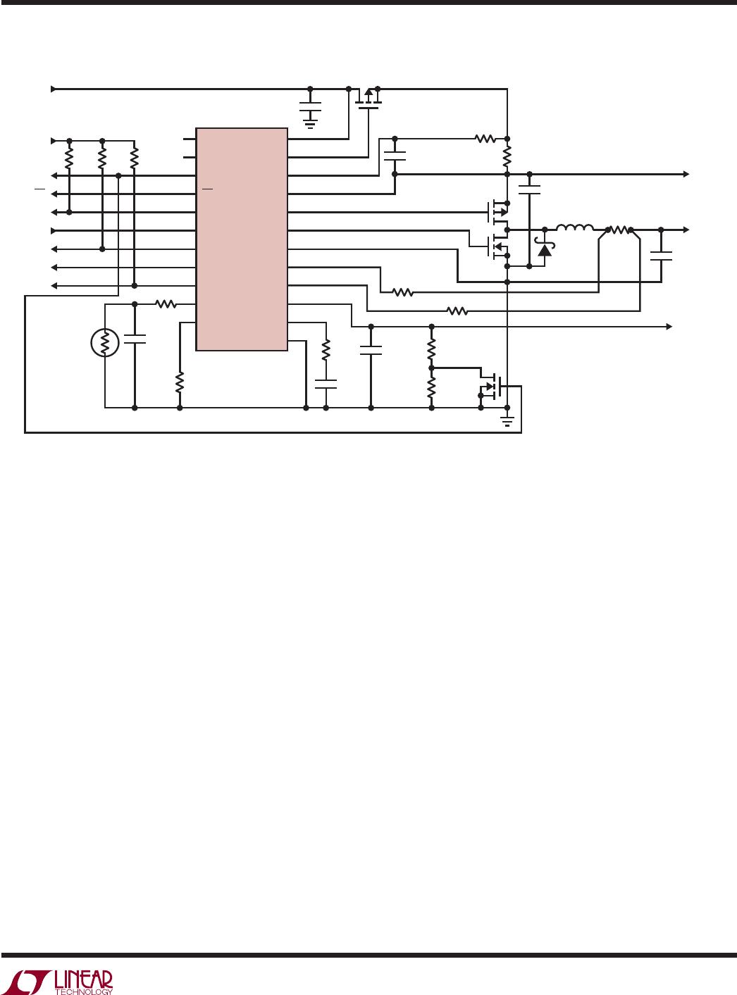
Conditioning Depleted Batteries
Severely depleted batteries, with less than 2.5V/cell, should
be conditioned with a trickle charge to prevent possible
damage. This trickle charge is typically 10% of the 1C
rate of the battery. The LTC4007 can automatically trickle
charge depleted batteries using the circuit in Figure 11.
If the battery voltage is less than 2.5V/cell (2.44V/cell if
CHEM is low) then the LOBAT indicator will be low and Q4
is off. This programs the charging current with R
PROG
= R6
+ R14. Charging current is approximately 300mA. When
the cell voltage becomes greater than 2.5V the LOBAT
indicator goes high, Q4 shorts out R13, then R
PROG
= R6.
Charging current is then equal to 3A.
PCB Layout Considerations
For maximum effi ciency, the switch node rise and fall
times should be minimized. To prevent magnetic and
electrical fi eld radiation and high frequency resonant
problems, proper layout of the components connected to
the IC is essential (see Figure 12). Here is a PCB layout
priority list for proper layout. Layout the PCB using this
specifi c order.
1. Input capacitors need to be placed as close as possible
to switching FET’s supply and ground connections.
Shortest copper trace connections possible. These
parts must be on the same layer of copper. Vias must
not be used to make this connection.
2. The control IC needs to be close to the switching FET’s
gate terminals. Keep the gate drive signals short for a
clean FET drive. This includes IC supply pins that connect
to the switching FET source pins. The IC can be placed
on the opposite side of the PCB relative to above.
3. Place inductor input as close as possible to switching
FET’s output connection. Minimize the surface area of
this trace. Make the trace width the minimum amount
needed to support current—no copper fi lls or pours.
Avoid running the connection using multiple layers in
parallel. Minimize capacitance from this node to any
other trace or plane.
4. Place the output current sense resistor right next to the
inductor output but oriented such that the IC’s current
sense feedback traces going to resistor are not long. The
feedback traces need to be routed together as a single
pair on the same layer at any given time with smallest
trace spacing possible. Locate any fi lter component on
these traces next to the IC and not at the sense resistor
location.
5. Place output capacitors next to the sense resistor output
and ground.
6. Output capacitor ground connections need to feed into
same copper that connects to the input capacitor ground
before tying back into system ground.