1
LT1115
1115fa
Ultralow Noise,
Low Distortion, Audio Op Amp
High Quality Audio Preamplifiers
Low Noise Microphone Preamplifiers
Very Low Noise Instrumentation Amplifiers
Low Noise Frequency Synthesizers
Infrared Detector Amplifiers
Hydrophone Amplifiers
Low Distortion Oscillators
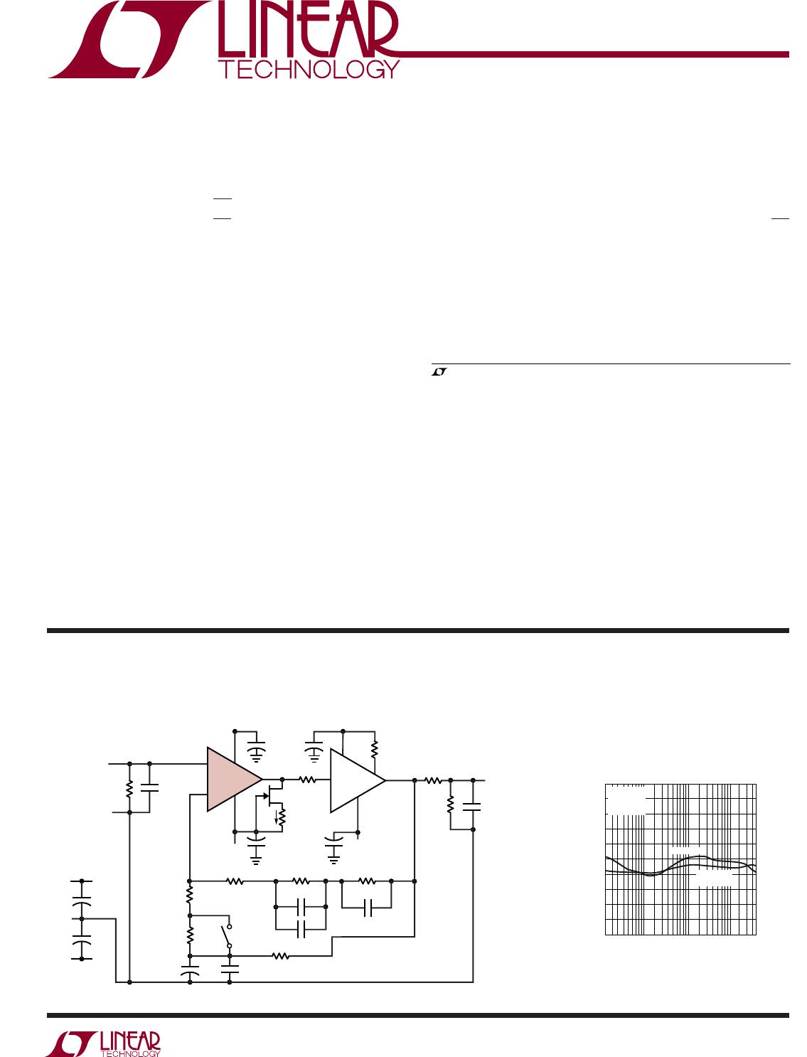
RIAA Phonograph Preamplifier (40/60db Gain)
Measured Deviation from RIAA
Response. lnput at 1kHz = 1mV
RMS
Pre-Emphasized
FREQUENCY (Hz)
20
–0.2000
DEVIATION (dB)
0.0
0.20000
0.40000
0.60000
100
1k 10k 50k
–0.4000
–0.6000
–0.8000
–1.000
0.80000
1.0000
V
S
= ± 18V
R
S
=25
T
A
=25
°
C
MEASURED
COMPUTER
SIMULATED
LT1115 • TA02
+
INPUT
(SELECT
PER
PHOTO
CART-
RIDGE)
COM
R
IN
47.5k (MM)
100 (MC)
C
IN
3
3
2
2
1
18V 18V
7
6
4
4
–18V
–18V
18V
V
+
V
–18V
1µF
35V
1µF
35V
470µF
35V
2200µF
16V
4.7µF
FILM
470µF
35V
1µF
35V
1µF
35V
100
49.9
562
499
22.6
330pF
15nF
5
2N4304*
~250
SELECT
FOR 2mA
RESISTORS 1%
*OR USE 2mA CURRENT SOURCE
MM = MOVING MAGNET
MC = MOVING COIL
BYPASS SUPPLIES WITH LOW ESR CAPS
OTHER CAPS: HIGH QUALITY FILM
NOTE:
2mA
17.8k
82.5k
210k
25k
210
3900pF
3900pF
SINGLE
POINT
BOARD
GROUND
OPEN—MM
CLOSED—MC
COM
R
L
R
BOOST
OUTPUT
A1
LT1115
A2
LT1010CT
LT1115 • TA01
+ +
+
+
+ +
+
FEATURES
APPLICATIO S
U
DESCRIPTIO
U
TYPICAL APPLICATIO
U
, LTC and LT are registered trademarks of Linear Technology Corporation.
Voltage Noise: 1.2nV/Hz Max at 1kHz
0.9nV/Hz Typ at 1kHz
Voltage and Current Noise 100% Tested
Gain-Bandwidth Product: 40MHz Min
Slew Rate: 10V/µs Min
Voltage Gain: 2 Million Min
Low THD at 10kHz, A
V
= –10, R
L
= 600: 0.002%
V
O
= 7V
RMS
Low IMD, CCIF Method, A
V
= +10: 0.002%
R
L
= 600
V
O
= 7V
RMS
The LT
®
1115 is the lowest noise audio operational ampli-
fier available. This ultralow noise performance (0.9nV/Hz
at 1kHz) is combined with high slew rates (>15V/µs) and
very low distortion specifications.
The RIAA circuit shown below using the LT1115 has very
low distortion and little deviation from ideal RIAA
response (see graph).
LT1115
2
1115fa
Operating Temperature Range ..................... 0°C to 70°C
Storage Temperature Range ..................65°C to 150°C
Lead Temperature (Soldering, 10 sec).................. 300°C
Supply Voltage ...................................................... ±22V
Differential Input Current (Note 5) ...................... ±25mA
Input Voltage ............................ Equal to Supply Voltage
Output Short-Circuit Duration .......................... Indefinite
(Note 1)
Consult LTC Marketing for parts specified with wider operating temperature ranges.
1
2
3
4
TOP VIEW
8
7
6
5
–IN
+IN
V
OUT
V
+
V
OS
TRIM
V
OS
TRIM
OVER-
COMP
N PACKAGE
8-LEAD PDIP
T
JMAX
= 115°C, θ
JA
= 130°C/W
ORDER
PART NUMBER
LT1115CN8
1
2
3
4
5
6
7
8
TOP VIEW
SW PACKAGE
16-LEAD PLASTIC SO
T
MAX
= 115°C, θ
JA
= 130°C/W
16
15
14
13
12
11
10
9
NC
NC
TRIM
–IN
+IN
V
NC
NC
NC
TRIM
V
+
OVERCOMP
NC
NC
NC
OUTPUT
LT1115CSW
ORDER
PART NUMBER
LT1115 • POI01
+
+
ABSOLUTE AXI U RATI GS
WWWU
U
PACKAGE DESCRIPTIO
ELECTRICAL CHARACTERISTICS
V
S
= ±18V, T
A
= 25°C, unless otherwise noted.
SYMBOL PARAMETER CONDITIONS MIN TYP MAX UNITS
THD Total Harmonic Distortion at 10kHz A
v
= –10, V
O
= 7V
RMS
, R
L
= 600 < 0.002 %
IMD Inter-Modulation Distortion (CCIF) A
v
= 10, V
O
= 7V
RMS
, R
L
= 600 < 0.0002 %
V
OS
Input Offset Voltage (Note 2) 50 200 µV
I
OS
Input Offset Current V
CM
= 0V 30 200 nA
I
B
Input Bias Current V
CM
= 0V ±50 ±380 nA
e
n
Input Noise Voltage Density f
o
= 10Hz 1.0 nV/Hz
f
o
= 1000Hz, 100% tested 0.9 1.2 nV/Hz
Wideband Noise DC to 20kHz 120 nV
RMS
Corresponding Voltage Level 136 dB
re 0.775V
i
n
Input Noise Current Density f
o
= 10Hz 4.7 pA/Hz
(Note 3) f
o
= 1000Hz, 100% tested 1.2 2.2 pA/Hz
Input Resistance
Common Mode 250 M
Differential Mode 15 k
Input Capacitance 5pF
Input Voltage Range ±13.5 ±15.0 V
3
LT1115
1115fa
SYMBOL PARAMETER CONDITIONS MIN TYP MAX UNITS
CMRR Common Mode Rejection V
CM
= ±13.5V 104 123 dB
Ratio
PSRR Power Supply Rejection V
S
= ±4V to ±19V 104 126 dB
Ratio
A
VOL
Large-Signal Voltage Gain R
L
2k, V
o
= ±14.5V 2.0 20 V/µV
R
L
1k, V
o
= ±13V 1.5 15 V/µV
R
L
600, V
o
= ±10V 1.0 10 V/µV
V
OUT
Maximum Output Voltage No Load ±15.5 ±16.5 V
Swing R
L
2k ±14.5 ±15.5 V
R
L
600 ±11.0 ±14.5 V
SR Slew Rate A
VCL
= –1 10 15 V/µs
GBW Gain-Bandwidth Product f
o
= 20kHz (Note 4) 40 70 MHz
Z
o
Open Loop 0utput Impedance V
o
= 0, I
o
= 0 70
I
S
Supply Current 8.5 11.5 mA
V
S
= ±18V, T
A
= 25°C, unless otherwise noted.
The
denotes specifications which apply over the full operating temperature range, otherwise specifications are at T
A
= 25°C.
V
S
= ±18V, unless otherwise noted.
SYMBOL PARAMETER CONDITIONS MIN TYP MAX UNITS
V
OS
Input Offset Voltage (Note 2) 75 280 µV
V
OS
/TAverage Input Offset Drift 0.5 µV/°C
I
OS
Input Offset Current V
CM
= 0V 40 300 nA
I
B
Input Bias Current V
CM
= 0V ±70 ±550 nA
Input Voltage Range ±13 ±14.8 V
CMRR Common Mode Rejection V
CM
= ±13V 100 120 dB
Ratio
PSRR Power Supply Rejection V
S
= ±4.5V to ±18V 100 123 dB
Ratio
A
VOL
Large-Signal Voltage Gain R
L
2k, V
o
= ±13V 1.5 15 V/µV
R
L
1k, V
o
= ±11V 1.0 10 V/µV
V
OUT
Maximum Output Voltage No Load ±15 ±16.3 V
Swing R
L
2k ±13.8 ±15.3 V
R
L
600 ±10 ±14.3 V
I
S
Supply Current 9.3 13 mA
Note 1: Absolute Maximum Ratings are those values beyond which the life
of a device may be impaired.
Note 2: Input Offset Voltage measurements are performed by automatic
test equipment approximately 0.5 sec after application of power.
Note 3: Current noise is defined and measured with balanced source
resistors. The resultant voltage noise (after subtracting the resistor noise
on an RMS basis) is divided by the sum of the two source resistors to
obtain current noise.
Note 4: Gain-bandwidth product is not tested. It is guaranteed by design
and by inference from the slew rate measurement.
Note 5: The inputs are protected by back-to-back diodes. Current limiting
resistors are not used in order to achieve low noise. If differential input
voltage exceeds ±1.8V, the input current should be limited to 25mA.
ELECTRICAL CHARACTERISTICS
LT1115CN8#PBF

Mfr. #:
Manufacturer:
Analog Devices Inc.
Description:
Precision Amplifiers Ultra Low Noise Audio OA
Lifecycle:
New from this manufacturer.
Delivery:
DHL FedEx Ups TNT EMS
Payment:
T/T Paypal Visa MoneyGram Western Union

Products related to this Datasheet