7
LT1115
1115fa
FPO
FPO
Small-Signal Transient Response
Maximum Output vs Frequency
(Power Bandwidth*)
FREQUENCY (Hz)
10k
0
PEAK-TO-PEAK OUTPUT VOLTAGE (V)
20
25
30
100k
1M 10M
15
10
5
V
S
= ±18V
T
A
= 25
°
C
R
L
= 2k
*POWER BANDWIDTH
f
P
= POWER BANDWIDTH
SLEW RATE
πE
OP
f
P
=
E
P
-
P
=
PEAK-TO-PEAK AMPLIFIER
OUTPUT VOLTAGE
LT1115 • TPC29
Closed-Loop Output Impedance
10
OUTPUT IMPEDANCE ()
1
10
100
100k
0.1
0.01
0.001
100
1k
10k
1M
I
O
= 1mA
V
S
= ±18V
T
A
= 25
°
C
FREQUENCY (Hz)
A
V
= 5
LT1115 • TPC30
A
V
= 1000
CCIF Testing
Note: The CCIF twin-tone intermodulation test inputs two closely
spaced equal amplitude tones to the device under test (DUT). The
analyzer then measures the intermodulation distortion (IMD)
produced in the DUT by measuring the difference tone equal to the
spacing between the tones.
The amplitude of the lMD test input is in sinewave peak equivalent
terms. As an example, selecting an amplitude of 1.000V will result in
the complex IMD signal having the same 2.828V peak-to-peak
amplitude that a 1.000V sinewave has. Clipping in a DUT will thus
occur at the same input amplitude for THD + N and IMD modes.
The LT1115 is a very high performance op amp, but
not necessarily one which is optimized for universal
application. Because of very low voltage noise and the
resulting high gain-bandwidth product, the device is most
applicable to relatively high gain applications. Thus, while
the LT1115 will provide notably superior performance to
the 5534 in most applications, the device may require
circuit modifications to be used at very low noise gains.
The part is not generally applicable for unity gain followers
or inverters. In general, it should always be used with good
low impedance bypass capacitors on the supplies, low
impedance feedback values, and minimal capacitive load-
ing. Ground plane construction is recommended, as is a
compact layout.
20mV/DIVISION
A
V
= –1,
R
S
= R
f
= 2k
C
f
= 30pF
C
L
= 80pF
0.2µs/DIVISION
TYPICAL PERFOR A CE CHARACTERISTICS
UW
Voltage Noise vs Current Noise
The LT1115’s less than 1nV/Hz voltage noise matches
that of the LT1028 and is three times better than the lowest
voltage noise heretofore available (on the LT1007/1037).
A necessary condition for such low voltage noise is
operating the input transistors at nearly 1mA of
collector currents, because voltage noise is inversely
proportional to the square root of the collector current.
Current noise, however, is directly proportional to the
square root of the collector current. Consequently, the
LT1115’s current noise is significantly higher than on
most monolithic op amps.
APPLICATIO S I FOR ATIO
WUUU
LT1115
8
1115fa
Therefore, to realize truly low noise performance it is
important to understand the interaction between voltage
noise (e
n
), current noise (i
n
) and resistor noise (r
n
).
Total Noise vs Source Resistance
The total input referred noise of an op amp is given by
e
t
= [e
n
2
+ r
n
2
+ (i
n
R
eq
)
2
]
1/2
where R
eq
is the total equivalent source resistance at
the two inputs
and r
n
= 4kTR
eq
= 0.13R
eq
in nV/Hz at 25°C
As a numerical example, consider the total noise at 1kHz
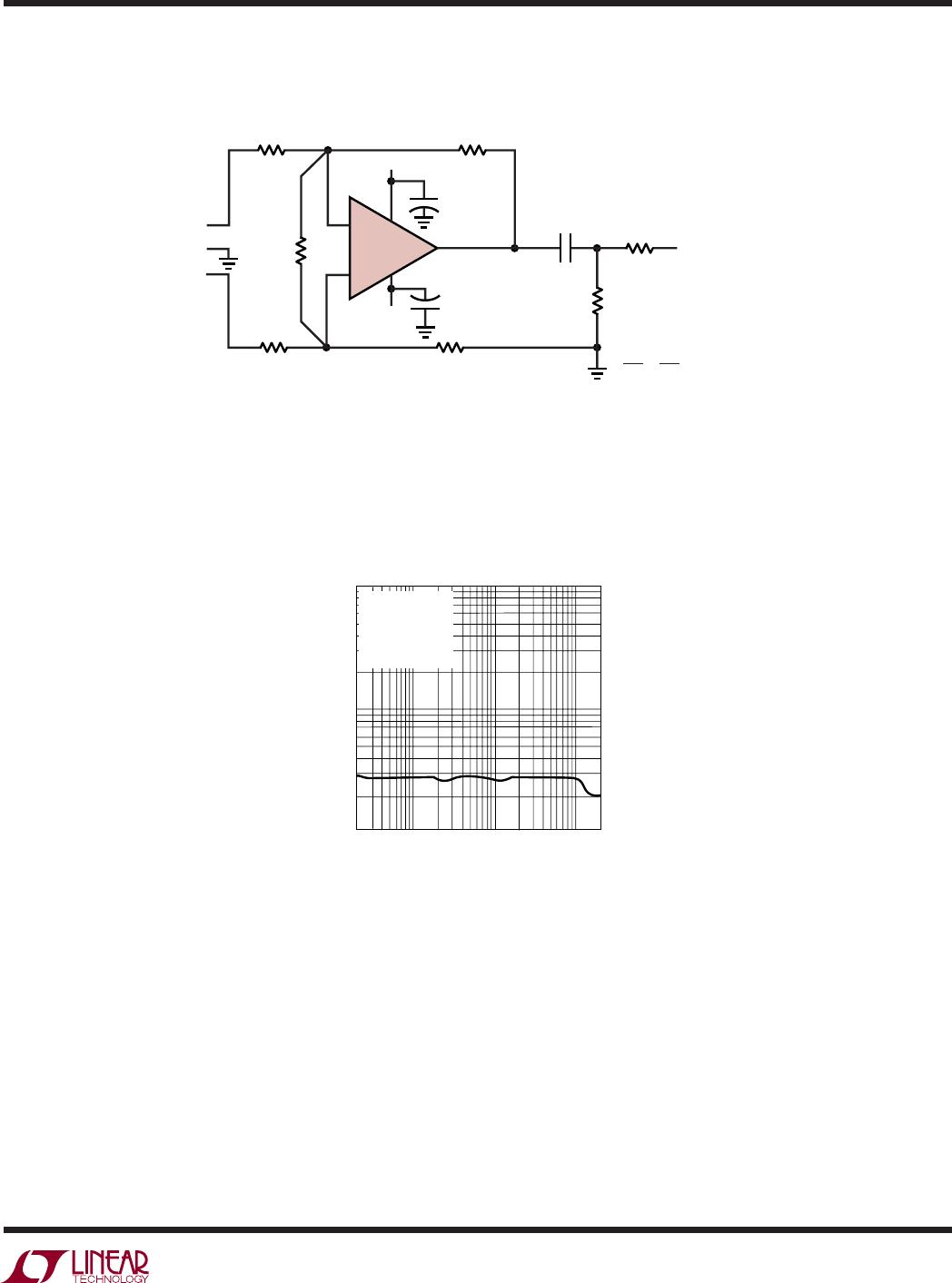
of the gain of 1000 amplifier shown below.
R
eq
= 100 + 100||100k 200
r
n
= 0.13200 = 1.84nV/Hz
e
n
= 0.85nV/Hz
i
n
= 1.0pA/Hz
e
t
= [0.85
2
+ 1.84
2
+ (1.0 x 2.0)
2
]
1/2
= 2.04nV/Hz
output noise = 1000 e
t
= 2.04µV/Hz
At very low source resistance (R
eq
< 40) voltage noise
dominates. As R
eq
is increased resistor noise becomes the
largest term—as in the example above—and the LT1115’s
voltage noise becomes negligible. As R
eq
is further
increased, current noise becomes important. At 1kHz,
when R
eq
is in excess of 20k, the current noise
component is larger than the resistor noise. The Total
Noise vs Matched Source Resistance plot in the Typical
Performance Characteristics section, illustrates the above
calculations.
+
100
100k
100
LT1115
LT1115 • AI01
The plot also shows that current noise is more dominant
at low frequencies, such as 10Hz. This is because resistor
noise is flat with frequency, while the 1/f corner of current
noise is typically at 250Hz. At 10Hz when R
eq
> 1k, the
current noise term will exceed the resistor noise.
When the source resistance is unmatched, the Total Noise
vs Unmatched Source Resistance plot should be con-
sulted. Note that total noise is lower at source resistances
below 1k because the resistor noise contribution is less.
When R
s
> 1k total noise is not improved, however. This
is because bias current cancellation is used to reduce
input bias current. The cancellation circuitry injects two
correlated current noise components into the two inputs.
With matched source resistors the injected current noise
creates a common-mode voltage noise and gets rejected
by the amplifier. With source resistance in one input only,
the cancellation noise is added to the amplifier’s inherent
noise.
In summary, the LT1115 is the optimum amplifier for
noise performance—provided that the source resistance
is kept low. The following table depicts which op amp
manufactured by Linear Technology should be used to
minimize noise—as the source resistance is increased
beyond the LT1115’s level of usefulness.
Best Op Amp for Lowest Total Noise vs Source Resistance
Note 1: Source resistance is defined as matched or unmatched, e.g.,
R
S
= 1k means: 1k at each input, or 1k at one input and zero at the
other.
SOURCE RESISTANCE BEST OP AMP
(NOTE 1) AT LOW FREQ (10Hz) WIDEBAND (1kHz)
0 to 400 LT1028/1115 LT1028/1115
400 to 4k LT1007/1037 LT1028/1115
4k to 40k LT1001* LT1007/1037
40k to 500k LT1012* LT1001*
500k to 5M LT1012* or LT1055 LT1012*
> 5M LT1055 LT1055
*These op amps are best utilized in applications requiring less bandwidth
than audio.
APPLICATIO S I FOR ATIO
WUUU
9
LT1115
1115fa
THD + Noise vs Frequency
(Figure 1)
Figure 1. Balanced Transformerless Microphone Preamp
FREQUENCY (Hz)
20
0.010
TOTAL HARMONIC DISTORTION + NOISE (%)
0.1
1
100
1k
20k
T
A
= 25
°
C
R
L
= 100k
V
IN
= 10mV
RMS
V
OUT
= 2.92V
RMS
R
S
= 150
LT1115 • TA04
+
1µF 35V
LOW ESR
1µF 35V
LOW ESR
R1
1k, 0.1%
R1
R2
1k, 0.1%
R2
R4
316k, 0.1%
R4
R3
316k, 0.1%
R3
INPUT
R
P
30k
1%
3
2
7
6
4
4.7µF
FILM
OUT
10k
1%
100
1%
18V
–18V
NOTE: MATCH RESISTOR PAIRS
TO ± 0.1%
LT1115
LT1115 • TA03
=
+
+
TYPICAL APPLICATIO S
U

LT1115CN8#PBF

Mfr. #:
Manufacturer:
Analog Devices Inc.
Description:
Precision Amplifiers Ultra Low Noise Audio OA
Lifecycle:
New from this manufacturer.
Delivery:
DHL FedEx Ups TNT EMS
Payment:
T/T Paypal Visa MoneyGram Western Union

Products related to this Datasheet