This is information on a product in full production.
October 2012 Doc ID 4980 Rev 8 1/16
16
74LCX125
Low-voltage CMOS quad bus buffer (3-state)
with 5 V tolerant inputs and outputs
Datasheet − production data
Features
■ 5 V tolerant inputs and outputs
■ High speed
–t
PD
= 5.2 ns (max.) at V
CC
= 3 V
■ Power-down protection on inputs and outputs
■ Symmetrical output impedance
–|I
OH
| = I
OL
= 24 mA (min.) at V
CC
= 3 V
■ PCI bus levels guaranteed at 24 mA
■ Balanced propagation delay
–t
PLH
≅ t
PHL
■
Operating voltage range
–V
CC
(opr.) = 2.0 V to 3.6 V
■ Pin and function compatible with 74 series 125
■ Latch-up performance exceeds 500 mA
(JESD 17)
■ ESD performance
– HBM: 2000 V (MIL STD 883 method 3015)
– MM: 200 V
– CDM: 1000 V
Applications
■ Automotive
■ Industrial
■ Computer
■ Consumer
Description
The 74LCX125 device is a low-voltage CMOS
quad bus buffer manufactured with sub-micron
silicon gate and double-layer metal wiring C
2
MOS
technology. It is ideal for low-power and high-
speed 3.3 V applications and can be interfaced to
a 5 V signal environment for both inputs and
outputs.
The device requires the 3-state control input G
to
be set high to place the output in the high
impedance state.
It has the same speed performance at 3.3 V as
the 5 V AC/ACT family, combined with lower
power consumption.
All inputs and outputs are equipped with
protection circuits against static discharge, giving
them 2 kV ESD immunity and transient excess
voltage.
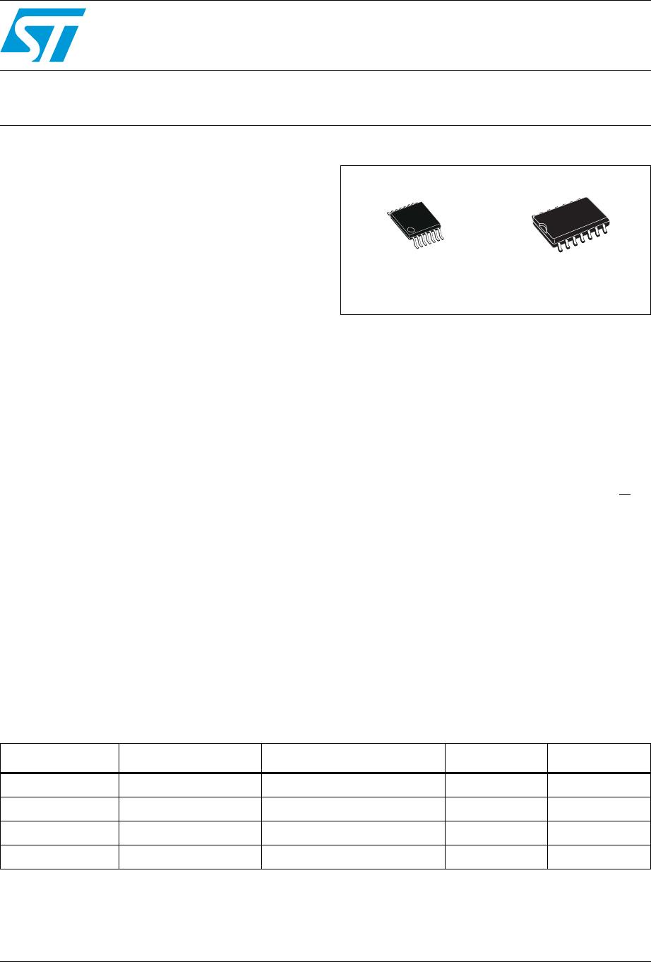
TSSOP14 SO-14
Table 1. Device summary
Order code Temperature range Package Packaging Marking
74LCX125TTR -40/+85 °C TSSOP14 Tape and reel LCX125
74LCX125YTTR
(1)
-40/+85 °C TSSOP14 (automotive grade) Tape and reel LCX125Y
74LCX125MTR -40/+85 °C SO-14 Tape and reel 74LCX125
74LCX125YMTR
(1)
-40/+85 °C SO-14 (automotive grade) Tape and reel 74LCX125Y
1. Qualification and characterization according to AEC Q100 and Q003 or equivalent, advanced screening according to AEC
Q001 and Q002 or equivalent.
www.st.com