74LCX125 Maximum ratings
Doc ID 4980 Rev 8 5/16
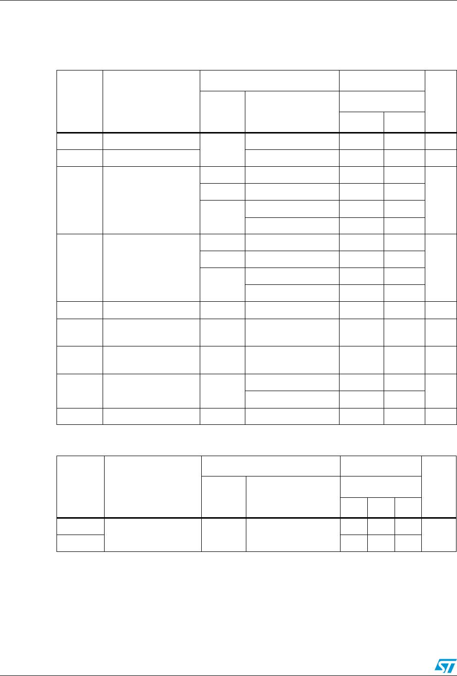
3 Maximum ratings
Stressing the device above the rating listed in Table 4: Absolute maximum ratings may
cause permanent damage to the device. These are stress ratings only and operation of the
device at these or any other conditions above those indicated in Table 5: Recommended
operating conditions of this specification is not implied. Exposure to absolute maximum
rating conditions for extended periods may affect device reliability.
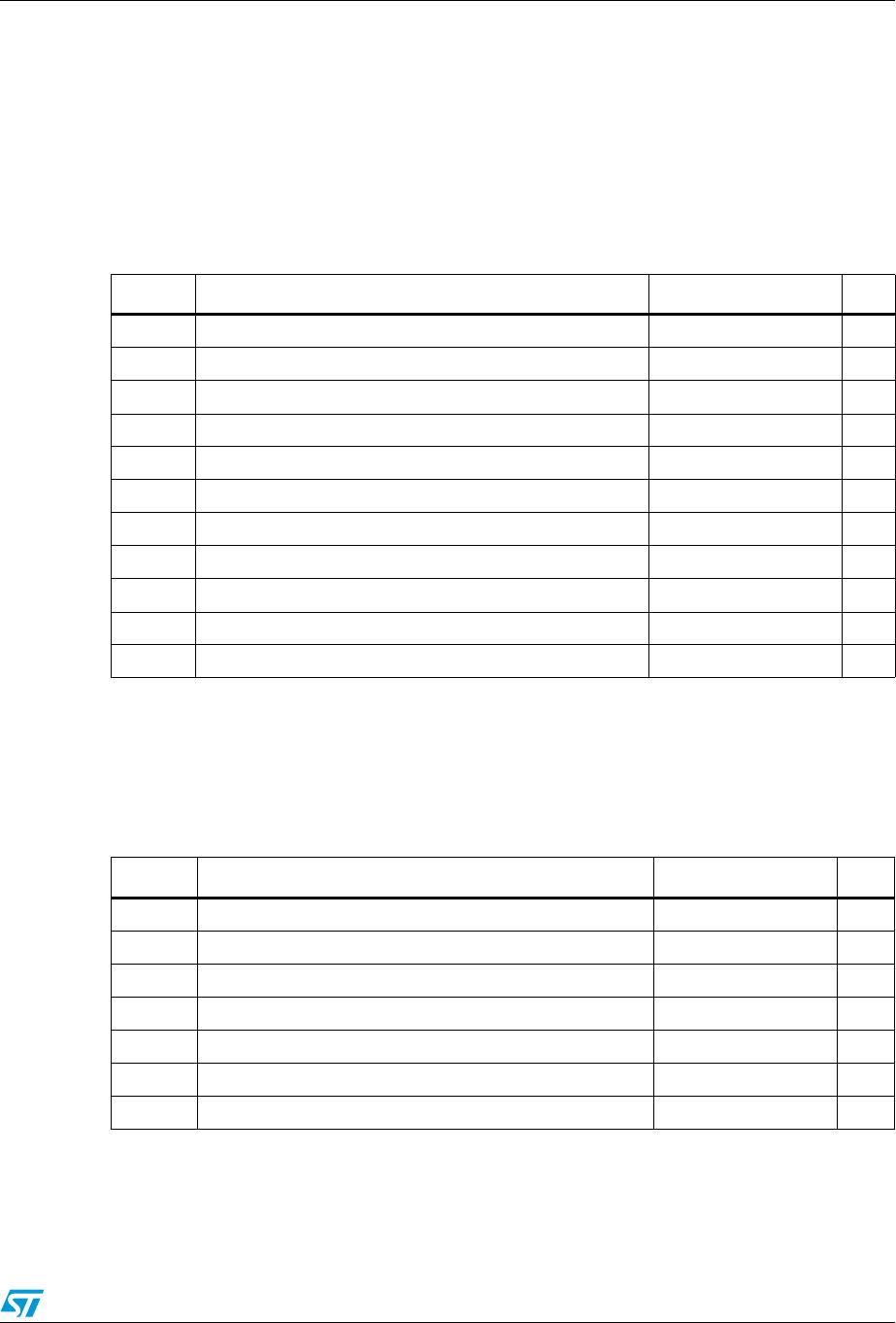
Recommended operating conditions
Table 4. Absolute maximum ratings
Symbol Parameter Value Unit
V
CC
Supply voltage -0.5 to +7.0 V
V
I
DC input voltage -0.5 to +7.0 V
V
O
DC output voltage (V
CC
= 0 V) -0.5 to +7.0 V
V
O
DC output voltage (high or low state)
(1)
1. I
O
absolute maximum rating must be observed.
-0.5 to V
CC
+ 0.5 V
I
IK
DC input diode current -50 mA
I
OK
DC output diode current
(2)
2. V
O
< GND.
-50 mA
I
O
DC output current ± 50 mA
I
CC
DC supply current per supply pin ± 100 mA
I
GND
DC ground current per supply pin ± 100 mA
T
stg
Storage temperature -65 to +150 °C
T
L
Lead temperature (10 sec.) 300 °C
Table 5. Recommended operating conditions
Symbol Parameter Value Unit
V
CC
Supply voltage
(1)
1. Truth table guaranteed: 1.5 V to 3.6 V.
2.0 to 3.6 V
V
I
Input voltage 0 to 5.5 V
V
O
Output voltage (V
CC
= 0 V) 0 to 5.5 V
V
O
Output voltage (high or low state) 0 to V
CC
V
I
OH
, I
OL
High or low level output current (V
CC
= 3.0 to 3.6 V) ± 24 mA
I
OH
, I
OL
High or low level output current (V
CC
= 2.7 V) ± 12 mA
dt/dv Input rise and fall time
(2)
2. V
IN
from 0.8 V to 2 V at V
CC
= 3.0 V.
0 to 10 ns/V