Addendum Automotive DDR3L SDRAM
MT41K128M8 – 16 Meg x 8 x 8 banks
MT41K64M16 – 8 Meg x 16 x 8 banks
Description
This addendum provides information to add Automo-
tive Ultra-high Temperature (AUT) option for the data
sheet. This addendum does not provide detailed infor-
mation about the device. Refer to the data sheet (1Gb:
x8, x16 Automotive DDR3L SDRAM, Rev. B 2/15 EN)
for a complete description of device functionality, op-
erating modes, and specifications for the same Micron
part number products. The 1.35V DDR3L SDRAM de-
vice is a low-voltage version of the 1.5V DDR3 SDRAM
device. Refer to the DDR3 (1.5V) SDRAM data sheet
specifications when running in 1.5V compatible
mode.
Features
• V
DD
= V
DDQ
= 1.35V (1.283V to 1.45V)
• Backward compatible to V
DD
= V
DDQ
= 1.5V ±0.075V
• Differential bidirectional data strobe
• 8n-bit prefetch architecture
• Differential clock inputs (CK, CK#)
• 8 internal banks
• Nominal and dynamic on-die termination (ODT)
for data, strobe, and mask signals
• Programmable CAS (READ) latency (CL)
• Programmable CAS additive latency (AL)
• Programmable CAS (WRITE) latency (CWL)
• Fixed burst length (BL) of 8 and burst chop (BC) of 4
(via the mode register set [MRS])
• Selectable BC4 or BL8 on-the-fly (OTF)
• Self refresh mode
• T
C
of –40°C to 125°C
– 64ms, 8192-cycle refresh at –40°C to 85°C
– 32ms at 85°C to 105°C
– 16ms at 105°C to 115°C
– 8ms at 115°C to 125°C
• Self refresh temperature (SRT)
• Automatic self refresh (ASR)
• Write leveling
• Multipurpose register
• Output driver calibration
• AEC-Q100
• PPAP submission
• 8D response time
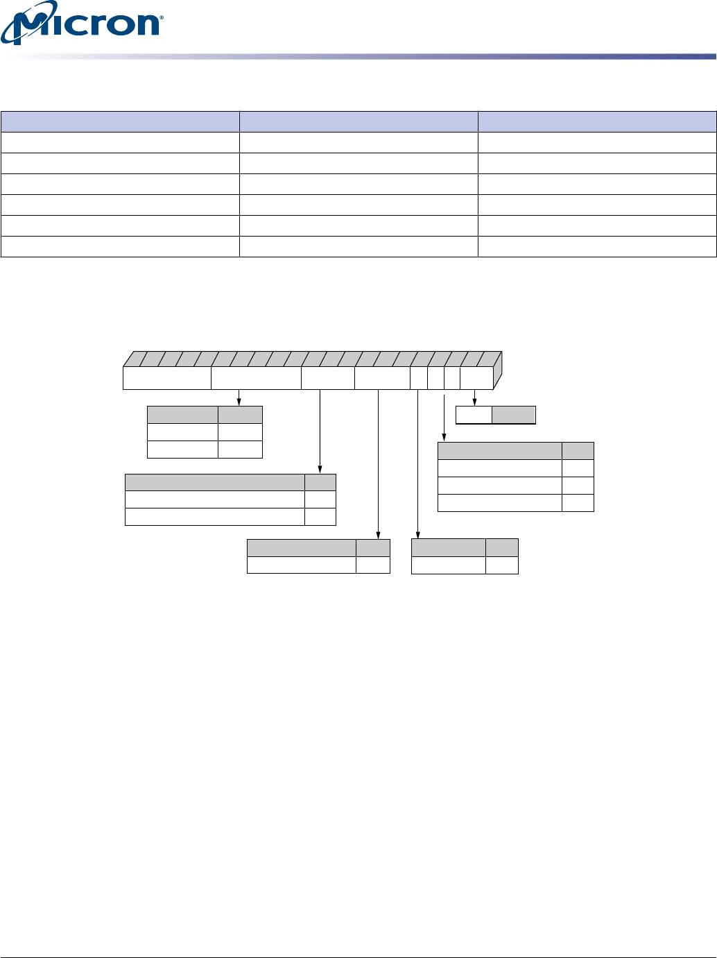
Options
1
Marking
• Configuration
– 128 Meg x 8 128M8
– 64 Meg x 16 64M16
• FBGA package (Pb-free) – x8
– 78-ball FBGA (8mm x 10.5mm) DA
• FBGA package (Pb-free) – x16
– 96-ball FBGA (8mm x 14mm) TW
• Timing – cycle time
– 1.07ns @ CL = 13 (DDR3-1866) -107
• Product certification
– Automotive A
• Operating temperature
– Industrial (–40°C ≤ T
C
≤ +95°C) IT
– Automotive (–40°C ≤ T
C
≤ +105°C) AT
– Ultra-high (–40°C ≤ T
C
≤ +125°C)
3
UT
• Revision :J
Notes:
1. Not all options listed can be combined to
define an offered product. Use the part
catalog search on http://www.micron.com
for available offerings.
2. The datasheet does not support ×4 mode
even though ×4 mode description exists in
the following sections.
3. The UT option use based on automotive us-
age model. Contact Micron sales represen-
tative for further information.
Table 1: Key Timing Parameters
Speed Grade Data Rate (MT/s) Target
t
RCD-
t
RP-CL
t
RCD (ns)
t
RP (ns) CL (ns)
-107 1866 13-13-13 13.91 13.91 13.91
1Gb: x8, x16 Automotive DDR3L SDRAM Addendum
Description
09005aef86775d6d
1gb_aut_DDR3L_1_35v_addendum.pdf - Rev. C 2/17 EN
1
Micron Technology, Inc. reserves the right to change products or specifications without notice.
© 2015 Micron Technology, Inc. All rights reserved.
Products and specifications discussed herein are subject to change by Micron without notice.