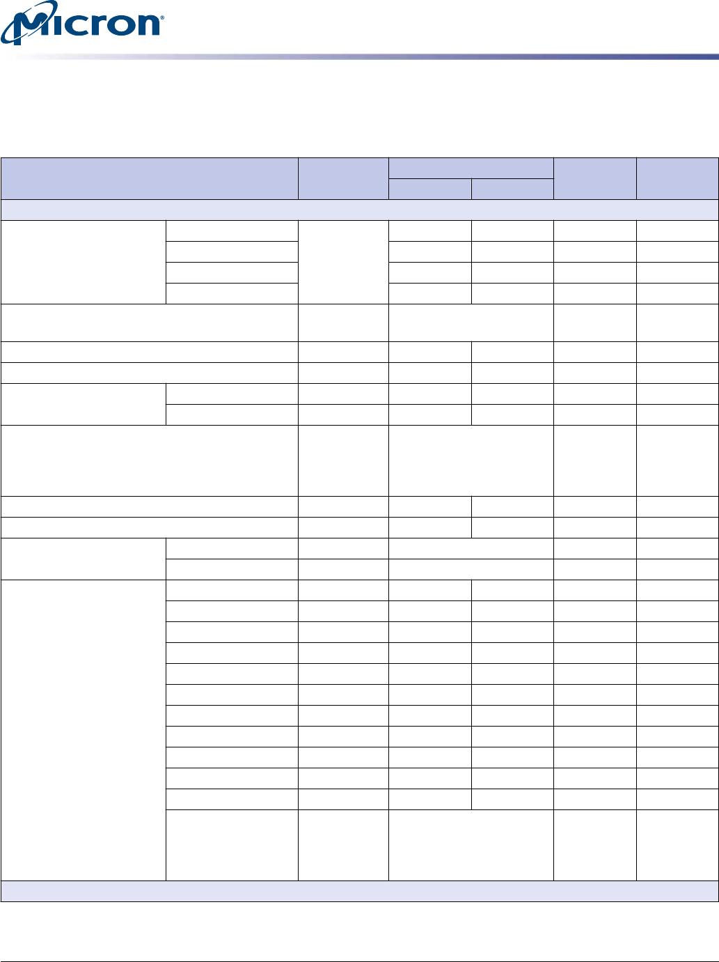
Electrical Characteristics – I
DD
Specifications
Table 6: I
DD
Maximum Limits
Parameter Symbol Width
DDR3L
-1866 Units Notes
Operating current 0: One bank ACTIVATE-to-PRE-
CHARGE
I
DD0
x8 36 mA 1, 2
x16 46 mA 1, 2
Operating current 1: One bank ACTIVATE-to-
READ-to-PRECHARGE
I
DD1
x8 47 mA 1, 2
x16 63 mA 1, 2
Precharge power-down current: Slow exit I
DD2P0
(slow) All 12 mA 1, 2, 6
Precharge power-down current: Fast exit I
DD2P1
(fast) All 12 mA 1, 2, 6
Precharge quiet standby I
DD2Q
All 15 mA 1, 2, 6
Precharge standby current I
DD2N
All 17 mA 1, 2, 6
Precharge standby ODT current I
DD2NT
x8 27 mA 1, 2, 6
x16 28 mA 1, 2, 6
Active power-down current I
DD3P
All 14 mA 1, 2, 6
Active standby current I
DD3N
x8 26 mA 1, 2, 6
x16 28 mA 1, 2, 6
Burst read operating current I
DD4R
x8 95 mA 1, 2
x16 135 mA 1, 2
Burst write operating current I
DD4W
x8 99 mA 1, 2
x16 149 mA 1, 2
Burst refresh current I
DD5B
All 165 mA 1, 2
Room temperature self refresh I
DD6
All 12 mA 1, 2, 3, 7
Extended temperature self refresh I
DD6ET
All 14 mA 1, 4, 7
All banks interleaved read current I
DD7
x8 162 mA 1, 2
x16 219 mA 1, 2
Reset current I
DD8
All 14 mA 1, 2
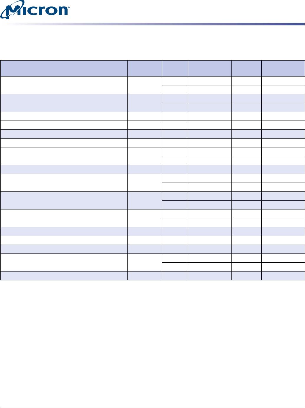
Notes:
1. T
C
= 85°C; SRT and ASR are disabled.
2. Enabling ASR could increase I
DD
x by up to an additional 2mA.
3. Restricted to T
C
(MAX) = 85°C.
4. T
C
= 85°C; ASR and ODT are disabled; SRT is enabled.
5. The I
DD
values must be derated (increased) on IT-option and AT-option devices when op-
erated outside of the range 0°C ≤ T
C
≤ +85°C:
5a. When T
C
< 0°C: I
DD2P0
, I
DD2P1
and I
DD3P
must be derated by 4%; I
DD4R
and I
DD4W
must
be derated by 2%; and I
DD6
and I
DD7
must be derated by 7%.
5b. When T
C
> 85°C: I
DD0
, I
DD1
, I
DD2N
, I
DD2NT
, I
DD2Q
, I
DD3N
, I
DD3P
, I
DD4R
, I
DD4W
, and I
DD5B
must be derated by 2%; I
DD2Px
must be derated by 30%.
6. The I
DD
values must be derated (increased) on UT-option. When T
C
> +105°C: I
DD2p0
,
I
DD2p1
, I
DD2N
, I
DD2NT
, I
DD2Q
, I
DD3P
, and I
DD3N
must be derated by 60% from the 85°C specs.
7. When T
C
>105°C, self refresh mode is not available.
1Gb: x8, x16 Automotive DDR3L SDRAM Addendum
Electrical Characteristics – I
DD
Specifications
09005aef86775d6d
1gb_aut_DDR3L_1_35v_addendum.pdf - Rev. C 2/17 EN
8
Micron Technology, Inc. reserves the right to change products or specifications without notice.
© 2015 Micron Technology, Inc. All rights reserved.