2008-2015 Microchip Technology Inc. DS80000425P-page 7
PIC18F24K20/25K20/44K20/45K20
19. Module: POR
The POR may release around 0.8V (below the
POR rearm voltage of 1.2V, nominal) when V
DD
rises from below 0.60V (when BOR is not enabled)
or 0.33V (when BOR is enabled).
Work around
Use Power-up Timer when operating with the EC,
EXTRC or HFINTOSC oscillator modes. Ensure
that VDD rise time is less than the Power-up Timer
time.
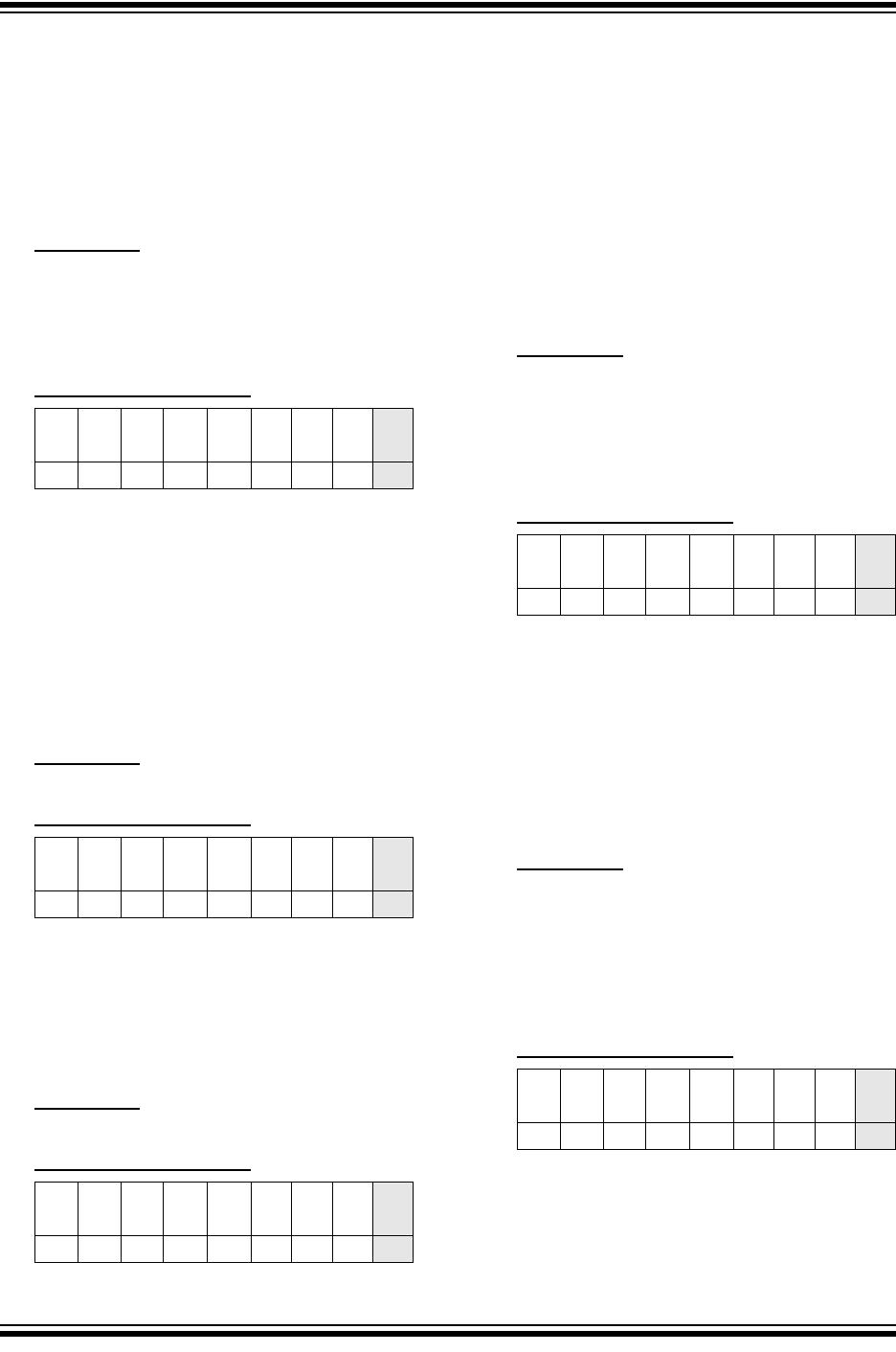
Affected Silicon Revisions
20. Module: POR
The part may hang in the Reset state when VDD
rises to the operating range at a rate faster than
7500V per second. Recovery from the hung state
is possible only by first lowering VDD to below 0.3V,
followed by raising V
DD to the operating range.
Work around
Slow VDD rise time by adding series resistance
between the voltage supply and the V
DD pin and
increasing the V
DD bypass capacitance. VDD
bypassing should remain on the pin side of the
series resistor.
Affected Silicon Revisions
21. Module: Clocks
EC mode operation is limited to a maximum of
48 MHz (Rev. A4 and A7 only).
Work around
Divide external clock by 4 and use HS-PLL Clock
mode for external clocking above 48 MHz.
Affected Silicon Revisions
22. Module: Comparators
When the CxON bit is clear, the output from the
comparator will be properly forced to zero, but the
CxPOL bit will improperly have no effect on the
CxOUT bit. This prevents presetting the compara-
tor change-on-interrupt mismatch latches as
described in the data sheet.
Work around
Configure one of the unused comparator input
channels as a digital output. Use that digital output
to manipulate the comparator output to the desired
CxOUT non-interrupt level. When the comparator
is then set to the desired inputs, the mismatch
latches will be preset to the non-interrupt level and
the CxIF flag can then be cleared.
Affected Silicon Revisions
23. Module: Data EEPROM Memory
The write/erase endurance of Data EE Memory is
limited to 10K cycles.
Work around
Use error correction method that stores data in
multiple locations.
Affected Silicon Revisions
24. Module: Program Flash Memory
The write/erase endurance of the PFM is limited to
1K cycles when V
DD is above 3V. Endurance
degrades when V
DD is below 3V.
Work around
For data tables in Program Flash Memory use
error correction method that stores data in multiple
locations.
Affected Silicon Revisions
0xA
0xC
0xE
0x11
0x16
0x18
0x19
0x1B
0x1C
XXXX
0xA
0xC
0xE
0x11
0x16
0x18
0x19
0x1B
0x1C
XXXX
0xA
0xC
0xE
0x11
0x16
0x18
0x19
0x1B
0x1C
XX
0xA
0xC
0xE
0x11
0x16
0x18
0x19
0x1B
0x1C
XXXX
0xA
0xC
0xE
0x11
0x16
0x18
0x19
0x1B
0x1C
XXXXXXX
0xA
0xC
0xE
0x11
0x16
0x18
0x19
0x1B
0x1C
XXXXXXX
PIC18F24K20/25K20/44K20/45K20
DS80000425P-page 8 2008-2015 Microchip Technology Inc.
25. Module: Configuration Bits
Bit 3 of CONFIG3H defaults to ‘0’ after a Bulk
Erase instead of ‘1’ as specified in the data sheet.
Work around
Program the HFOFST bit to the desired state after
a Bulk Erase. All MPLAB
®
IDE programming tools
currently perform this way.
Affected Silicon Revisions
26. Module: EUSART
In Asynchronous Receive mode, the RCIDL bit of
the BAUDCON register will properly go low when
an invalid Start bit less than 1/8th of a bit time is
received. The RCIDL bit will then stay low improp-
erly until a valid Start bit is received.
Work around
When monitoring the RCIDL bit, measure the
length of time between the RCIDL going low and
the RCIF flag going high. If this time is greater than
one character time, then restore the RCIDL bit by
resetting the EUSART module. The EUSART
module is reset when the SPEN bit of the RCSTA
register is cleared.
Affected Silicon Revisions
27. Module: PORTB
Setting a PORTB interrupt-on-change enable bit of
the IOCB register while the corresponding PORTB
input is high will cause an RBIF interrupt.
Work around
Set the IOCB bits to the desired configuration, then
read PORTB to clear the mismatch latches.
Finally, clear the RBIF bit before setting the RBIE
bit.
Affected Silicon Revisions
28. Module: ADC
After extended stress, the Most Significant bit
(MSb) of the ADC conversion result can become
stuck at ‘0’. Conversions resulting in code 511 or
less are still accurate, but conversions that should
result in codes greater than 511 are, instead,
pinned at 511.
The potential for failures is a function of several
factors:
The potential for failures increases over the life
of the part. No failures have ever been seen for
accelerated stress estimated to be equivalent
to 34 years at room temperature. The failure
rate after accelerated stress estimated to be
equivalent to 146 years at room temperature
can be as high as 10% for V
DD = 1.8V. The time
to failure will decrease as the operating
temperature increases.
The potential for failures is highest at low V
DD
and decreases as V
DD increases.
Work around
1. Restrict the input voltage to less than 1/2 of the
ADC voltage reference so that the expected
result is always a code less than or equal to 511.
2. Use manual acquisition time (ACQT<2:0> =
000) and put the part to Sleep after each
conversion.
Affected Silicon Revisions
29. Module: ECCP
Changing direction in Full-Bridge mode inserts a
dead-band time of 4/F
OSC * TMR2 Prescale
instead of 1/F
OSC * TMR2 Prescale as specified in
the data sheet.
Work around
None.
Affected Silicon Revisions
0xA
0xC
0xE
0x11
0x16
0x18
0x19
0x1B
0x1C
XXXX
0xA
0xC
0xE
0x11
0x16
0x18
0x19
0x1B
0x1C
XXXX
0xA
0xC
0xE
0x11
0x16
0x18
0x19
0x1B
0x1C
XXXXXXXXX
0xA
0xC
0xE
0x11
0x16
0x18
0x19
0x1B
0x1C
XXXXXXX
0xA
0xC
0xE
0x11
0x16
0x18
0x19
0x1B
0x1C
XXXXXXXXX
2008-2015 Microchip Technology Inc. DS80000425P-page 9
PIC18F24K20/25K20/44K20/45K20
30. Module: ECCP
ECCP – In Full-Bridge mode when PR2 =
CCPR1L and DC1B[1:0] <>‘00’ and the direction
is changed, then the dead time before the modu-
lated output starts is compromised. The modulated
signal improperly starts immediately with the direc-
tion change and stays on for T
OSC *TMR2
Prescale * DC1B[1:0].
Work around
Avoid changing direction when the duty cycle is
within three Least Significant steps of 100% duty
cycle. Instead, clear the DC1B[1:0] bits before the
direction change and then set them to the desired
value after the direction change is complete.
Affected Silicon Revisions
31. Module: MSSP SPI
When the SPI clock is configured for Timer2/2
(SSPCON1<3:0> = 0011) and the CKE bit of the
SSPSTAT register is ‘1’, then when SSPBUF is
written, the SCK output is improperly immediately
driven to the non-Idle state together with the MSb
value of the SSPBUF. The duration at which SDO
and SCK remain at these levels may be shorter
than a full half-bit period. The remaining bits in the
byte are output properly.
Work around
None.
Affected Silicon Revisions
32. Module: MSSP SPI
In SPI Master mode, when the CKE bit of the
SSPSTAT register is cleared and the SMP bit of
the SSPSTAT register is set, then the last bit of the
incoming data stream (bit 0) at the SDI pin will not
be sampled properly.
Work around
None.
Affected Silicon Revisions
33. Module: MSSP SPI
In SPI Master mode, if the SSPBUF register is
written while a byte is actively being transmitted,
an extra clock pulse will be improperly generated
at the end of the transmission. Further writes to the
SSPBUF register will be inhibited although 8 or 9
clock pulses will be generated for each attempted
write. The WCON bit of the SSPCON register is
properly set indicating that a write collision
occurred. However, the write collision condition
can only be cleared by resetting the MSSP
module. Clear the MSSP by clearing the SSPEN
bit of the SSPCON1 register.
Work around
Use the SSPIF bit of the PIR1 register or the BF bit
of the SSPSTAT register to determine that the
transmission is complete before writing the
SSPBUF register. In the event that a write collision
does occur, use the slave select feature to
resynchronize the slave clock.
Affected Silicon Revisions
34. Module: MSSP I
2
C
In Master I
2
C Receive mode if a Stop condition
occurs in the middle of an address or data
reception, then the SCL clock stream will continue
endlessly and the RCEN bit of the SSPCON2
register will remain set improperly. If a Start
condition occurs after the improper Stop condition
then nine additional clocks will be generated
followed by the RCEN bit going low.
Work around
Use low-impedance pull-ups on the SDA line to
reduce the possibility of noise glitches which may
trigger an improper Stop event. Use a time-out
event timer to detect the unexpected Stop
condition and resulting stuck RCEN bit. Clear the
stuck RCEN bit by clearing the SSPEN bit of
SSPCON1.
Affected Silicon Revisions
0xA
0xC
0xE
0x11
0x16
0x18
0x19
0x1B
0x1C
XXXXXXXXX
0xA
0xC
0xE
0x11
0x16
0x18
0x19
0x1B
0x1C
XXXXXXXXX
0xA
0xC
0xE
0x11
0x16
0x18
0x19
0x1B
0x1C
XXXXXXXXX
0xA
0xC
0xE
0x11
0x16
0x18
0x19
0x1B
0x1C
XXXXXXXXX
0xA
0xC
0xE
0x11
0x16
0x18
0x19
0x1B
0x1C
XXXXXXXXX

PIC18F24K20-E/SS

Mfr. #:
Manufacturer:
Microchip Technology
Description:
8-bit Microcontrollers - MCU 16KB Flash 768B RAM 25 I/O 8B
Lifecycle:
New from this manufacturer.
Delivery:
DHL FedEx Ups TNT EMS
Payment:
T/T Paypal Visa MoneyGram Western Union