ADF4113HV Data Sheet
Rev. B | Page 2 of 20
TABLE OF CONTENTS
Features .............................................................................................. 1
Applications ....................................................................................... 1
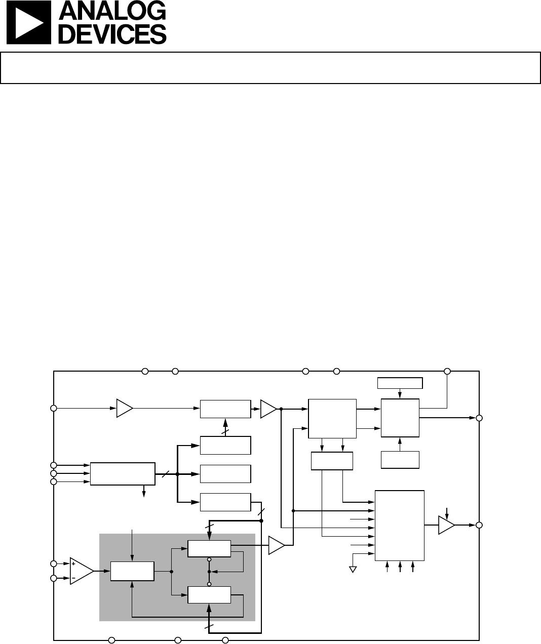
Functional Block Diagram .............................................................. 1
Revision History ............................................................................... 2
Specifications ..................................................................................... 3
Timing Characteristics ................................................................ 4
Absolute Maximum Ratings ............................................................ 5
Transistor Count ........................................................................... 5
Thermal Resistance ...................................................................... 5
ESD Caution .................................................................................. 5
Pin Configurations and Function Descriptions ........................... 6
Typical Performance Characteristics ............................................. 7
Circuit Description ........................................................................... 9
Reference Input Section ............................................................... 9
RF Input Stage ............................................................................... 9
Prescaler (P/P + 1) ........................................................................9
A and B Counters ..........................................................................9
R Counter .......................................................................................9
Phase Frequency Detector (PFD) and Charge Pump ............ 10
Muxout and Lock Detect ........................................................... 10
Input Shift Register .................................................................... 10
Function Latch ............................................................................ 13
Applications ..................................................................................... 15
Using a Digitial-to-Analog Converter to Drive
the R
SET
Pin .................................................................................. 15
Interfacing ................................................................................... 15
PCB Design Guidelines for Chip Scale Package .................... 16
Outline Dimensions ....................................................................... 17
Ordering Guide .......................................................................... 17
REVISION HISTORY
10/12—Rev. A to Rev. B
Changed CP-20-1 Package to CP-20-6 Package ............. Universal
Changes to Table 3 and Table 4 ....................................................... 5
Added EPAD Notation..................................................................... 6
Updated Outline Dimensions ....................................................... 17
Changes to Ordering Guide .......................................................... 17
9/08—Rev. 0 to Rev. A
Changes to Figure 22 ...................................................................... 13
1/07—Revision 0: Initial Version