LTC3108
1
3108fc
For more information www.linear.com/LTC3108
Typical applicaTion
DescripTion
Ultralow Voltage Step-Up
Converter and Power Manager
The LT C
®
3108 is a highly integrated DC/DC converter ideal
for harvesting and managing surplus energy from extremely
low input voltage sources such as TEGs (thermoelectric
generators), thermopiles and small solar cells. The step-up
topology operates from input voltages as low as 20mV.
The LTC3108 is functionally equivalent to the LTC3108-1
except for its unique fixed V
OUT
options.
Using a small step-up transformer, the LTC3108 provides a
complete power management solution for wireless sensing
and data acquisition. The 2.2V LDO powers an external
microprocessor, while the main output is programmed to
one of four fixed voltages to power a wireless transmitter
or sensors. The power good indicator signals that the main
output voltage is within regulation. A second output can be
enabled by the host. A storage capacitor provides power
when the input voltage source is unavailable. Extremely
low quiescent current and high efficiency design ensure
the fastest possible charge times of the output reservoir
capacitor.
The LTC3108 is available in a small, thermally enhanced
12-lead (3mm × 4mm) DFN package and a 16-lead SSOP
package.
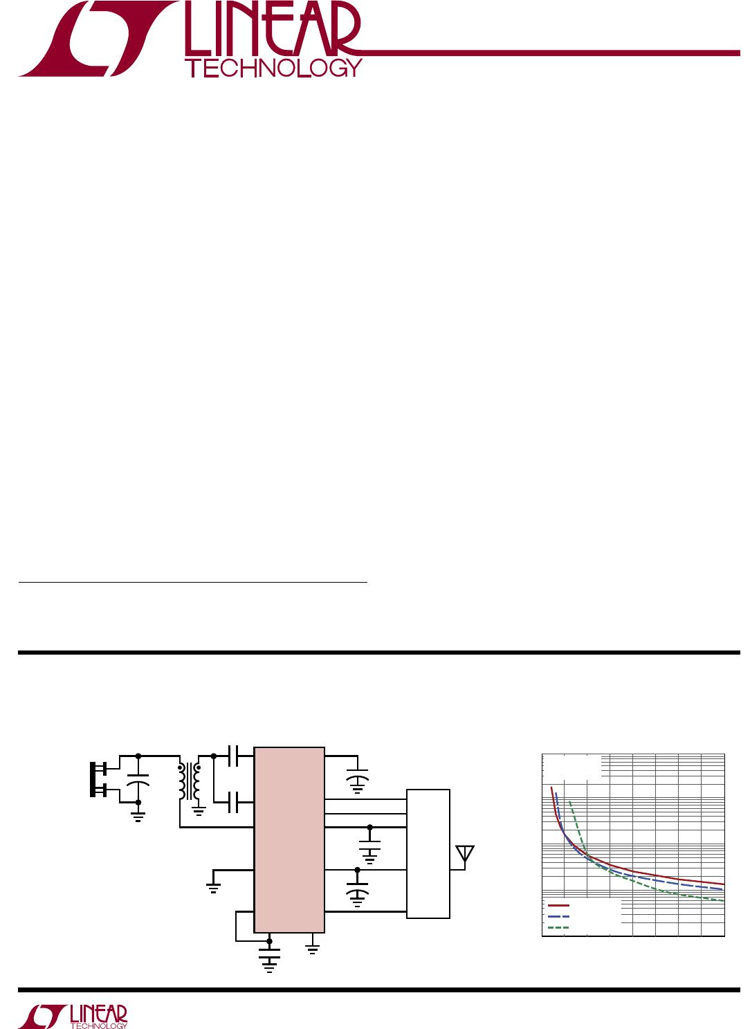
Wireless Remote Sensor Application Powered From a Peltier Cell
FeaTures
applicaTions
n
Operates from Inputs of 20mV
n
Complete Energy Harvesting Power
Management System
- Selectable V
OUT
of 2.35V, 3.3V, 4.1V or 5V
- LDO: 2.2V at 3mA
- Logic Controlled Output
- Reserve Energy Output
n
Power Good Indicator
n
Uses Compact Step-Up Transformers
n
Small 12-Lead (3mm × 4mm) DFN or 16-Lead
SSOP Packages
n
Remote Sensors and Radio Power
n
Surplus Heat Energy Harvesting
n
HVAC Systems
n
Industrial Wireless Sensing
n
Automatic Metering
n
Building Automation
n
Predictive Maintenance
3108 TA01a
C1
20mV TO 500mV
C2
SW
VS2
VS1
V
OUT2
PGOOD
2.2V
470µF
PGD
VLDO
VSTORE
+
V
OUT
V
OUT2_EN
LTC3108
VAUX GND
0.1F
6.3V
5V
3.3V
F
1nF
220µF
1:100
330pF
SENSORS
RF LINK
µP
2.2µF
+
+
+
THERMOELECTRIC
GENERATOR
V
OUT
Charge Time
L, LT, LTC, LTM, Linear Technology and the Linear logo are registered trademarks of Linear
Technology Corporation. All other trademarks are the property of their respective owners.
V
IN
(mV)
TIME (sec)
10
1
100
1000
0
3108 TA01b
0
100 150 250
50
200 300 350 400
V
OUT
= 3.3V
C
OUT
= 470µF
1:100 Ratio
1:50 Ratio
1:20 Ratio
LTC3108
2
3108fc
For more information www.linear.com/LTC3108
absoluTe MaxiMuM raTings
SW Voltage ..................................................–0.3V to 2V
C1 Voltage .................................................... –0.3V to 6V
C2 Voltage (Note 5) ......................................... –8V to 8V
V
OUT2
, V
OUT2_EN
........................................... –0.3V to 6V
VAUX ....................................................15mA into VAUX
(Note 1)
12
11
10
9
8
7
13
GND
1
2
3
4
5
6
SW
C2
C1
V
OUT2_EN
VS1
VS2
VAUX
VSTORE
V
OUT
V
OUT2
VLDO
PGD
TOP VIEW
DE PACKAGE
12-LEAD (4mm × 3mm) PLASTIC DFN
T
JMAX
= 125°C, θ
JA
= 43°C/W
EXPOSED PAD (PIN 13) IS GND, MUST BE SOLDERED TO PCB (NOTE 4)
GN PACKAGE
16-LEAD PLASTIC SSOP NARROW
1
2
3
4
5
6
7
8
TOP VIEW
16
15
14
13
12
11
10
9
GND
VAUX
VSTORE
V
OUT
V
OUT2
VLDO
PGD
GND
GND
SW
C2
C1
V
OUT2_EN
VS1
VS2
GND
T
JMAX
= 125°C, θ
JA
= 110°C/W
pin conFiguraTion
elecTrical characTerisTics
PARAMETER CONDITIONS MIN TYP MAX UNITS
Minimum Start-Up Voltage Using 1:100 Transformer Turns Ratio, VAUX = 0V 20 50 mV
No-Load Input Current Using 1:100 Transformer Turns Ratio; V
IN
= 20mV,
V
OUT2_EN
= 0V; All Outputs Charged and in Regulation
3 mA
Input Voltage Range Using 1:100 Transformer Turns Ratio
l
V
STARTUP
500 mV
The l denotes the specifications which apply over the full operating
junction temperature range, otherwise specifications are for T
A
= 25°C (Note 2). VAUX = 5V, unless otherwise noted.
orDer inForMaTion
LEAD FREE FINISH TAPE AND REEL PART MARKING* PACKAGE DESCRIPTION TEMPERATURE RANGE
LTC3108EDE#PBF LTC3108EDE#TRPBF 3108 12-Lead (4mm × 3mm) Plastic DFN –40°C to 125°C
LTC3108IDE#PBF LTC3108IDE#TRPBF 3108 12-Lead (4mm × 3mm) Plastic DFN –40°C to 125°C
LTC3108EGN#PBF LTC3108EGN#TRPBF 3108 16-Lead Plastic SSOP –40°C to 125°C
LTC3108IGN#PBF LTC3108IGN#TRPBF 3108 16-Lead Plastic SSOP –40°C to 125°C
Consult LTC Marketing for parts specified for other fixed output voltages or wider operating temperature ranges.
*The temperature grade is identified by a label on the shipping container.
For more information on lead free part marking, go to: http://www.linear.com/leadfree/
For more information on tape and reel specifications, go to: http://www.linear.com/tapeandreel/
VS1, VS2, VAUX, V
OUT
, PGD ........................–0.3V to 6V
VLDO, VSTORE ............................................–0.3V to 6V
Operating Junction Temperature Range
(Note 2) ................................................. –40°C to 125°C
Storage Temperature Range .................. –65°C to 125°C
LTC3108
3
3108fc
For more information www.linear.com/LTC3108
Note 1: Stresses beyond those listed under Absolute Maximum Ratings
may cause permanent damage to the device. Exposure to any Absolute
Maximum Rating condition for extended periods may affect device
reliability and lifetime.
Note 2: The LTC3108 is tested under pulsed load conditions such that T
J
T
A
. The LTC3108E is guaranteed to meet specifications from 0°C to 85°C
junction temperature. Specifications over the –40°C to 125°C operating
junction temperature range are assured by design, characterization and
correlation with statistical process controls. The LTC3108I is guaranteed
over the full –40°C to 125°C operating junction temperature range.
Note that the maximum ambient temperature is determined by specific
operating conditions in conjunction with board layout, the rated thermal
package thermal resistance and other environmental factors. The junction
temperature (T
J
) is calculated from the ambient temperature (T
A
) and
power dissipation (P
D
) according to the formula: T
J
= T
A
+ (P
D
θ
JA
°C/W),
where θ
JA
is the package thermal impedance.
Note 3: Specification is guaranteed by design and not 100% tested in
production.
Note 4: Failure to solder the exposed backside of the package to the PC
board ground plane will result in a thermal resistance much higher than
43°C/W.
Note 5: The absolute maximum rating is a DC rating. Under certain
conditions in the applications shown, the peak AC voltage on the C2 pin
may exceed ±8V. This behavior is normal and acceptable because the
current into the pin is limited by the impedance of the coupling capacitor.
elecTrical characTerisTics
The l denotes the specifications which apply over the full operating
junction temperature range, otherwise specifications are for T
A
= 25°C (Note 2). VAUX = 5V, unless otherwise noted.
PARAMETER CONDITIONS MIN TYP MAX UNITS
Output Voltage VS1 = VS2 = GND
VS1 = VAUX, VS2 = GND
VS1 = GND, VS2 = VAUX
VS1 = VS2 = VAUX
l
l
l
l
2.30
3.234
4.018
4.90
2.350
3.300
4.100
5.000
2.40
3.366
4.182
5.10
V
V
V
V
V
OUT
Quiescent Current V
OUT
= 3.3V, V
OUT2_EN
= 0V 0.2 µA
VAUX Quiescent Current No Load, All Outputs Charged 6 9 µA
LDO Output Voltage 0.5mA Load
l
2.134 2.2 2.266 V
LDO Load Regulation For 0mA to 2mA Load 0.5 1 %
LDO Line Regulation For VAUX from 2.5V to 5V 0.05 0.2 %
LDO Dropout Voltage I
LDO
= 2mA
l
100 200 mV
LDO Current Limit V
LDO
= 0V
l
4 11 mA
V
OUT
Current Limit V
OUT
= 0V
l
2.8 4.5 7 mA
VSTORE Current Limit VSTORE = 0V
l
2.8 4.5 7 mA
VAUX Clamp Voltage Current into VAUX = 5mA
l
5 5.25 5.55 V
VSTORE Leakage Current VSTORE = 5V 0.1 0.3 µA
V
OUT2
Leakage Current V
OUT2
= 0V, V
OUT2_EN
= 0V 0.1 µA
VS1, VS2 Threshold Voltage
l
0.4 0.85 1.2 V
VS1, VS2 Input Current VS1 = VS2 = 5V 0.01 0.1 µA
PGOOD Threshold (Rising) Measured Relative to the V
OUT
Voltage –7.5 %
PGOOD Threshold (Falling) Measured Relative to the V
OUT
Voltage –9 %
PGOOD V
OL
Sink Current = 100µA 0.15 0.3 V
PGOOD V
OH
Source Current = 0 2.1 2.2 2.3 V
PGOOD Pull-Up Resistance 1
V
OUT2_EN
Threshold Voltage V
OUT2_EN
Rising
l
0.4 1 1.3 V
V
OUT2_EN
Pull-Down Resistance 5
V
OUT2
Turn-On Time 5 µs
V
OUT2
Turn-Off Time (Note 3) 0.15 µs
V
OUT2
Current Limit V
OUT
= 3.3V
l
0.15 0.3 0.45 A
V
OUT2
Current Limit Response Time (Note 3) 350 ns
V
OUT2
P-Channel MOSFET On-Resistance V
OUT
= 3.3V (Note 3) 1.3 Ω
N-Channel MOSFET On-Resistance C2 = 5V (Note 3) 0.5 Ω
LTC3108EDE#PBF

Mfr. #:
Manufacturer:
Analog Devices / Linear Technology
Description:
Switching Voltage Regulators Ultralow Voltage Step-Up Converter and Power Manager
Lifecycle:
New from this manufacturer.
Delivery:
DHL FedEx Ups TNT EMS
Payment:
T/T Paypal Visa MoneyGram Western Union