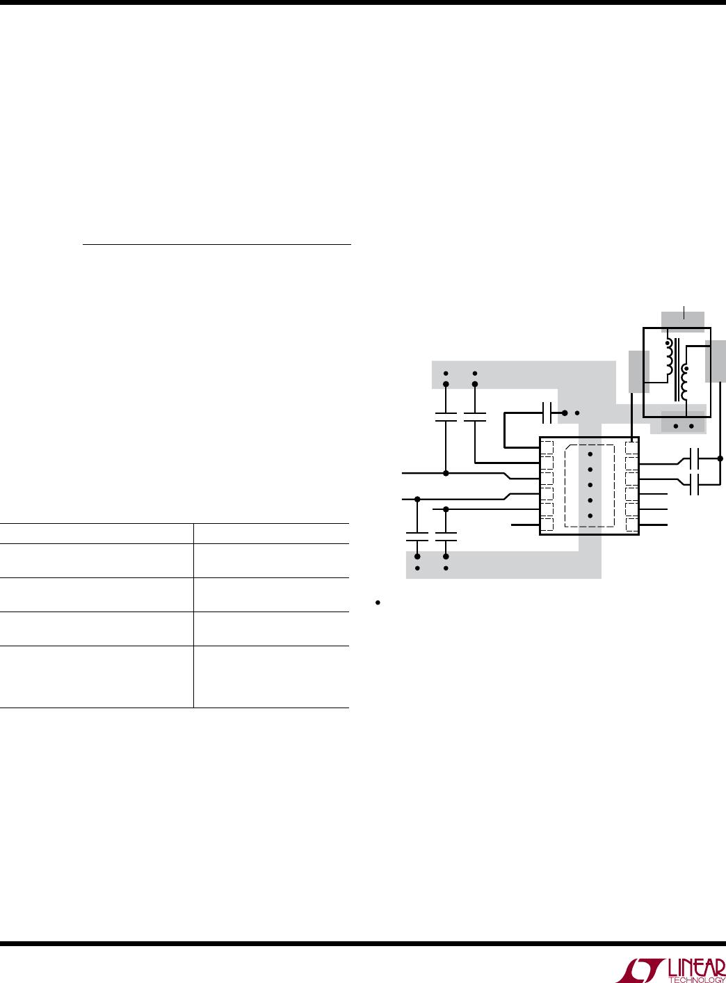
LTC3108
17
3108fc
For more information www.linear.com/LTC3108
applicaTions inForMaTion
at which the load pulses can occur for a given output cur-
rent from the LTC3108 will also be shown.
In this example, V
OUT
is set to 3.3V, and the maximum
allowed voltage droop during a transmit burst is 10%, or
0.33V. The duration of a transmit burst is 1ms, with a total
average current requirement of 40mA during the burst.
Given these factors, the minimum required capacitance
on V
OUT
is:
C(µF)
121µF
OUT
Note that this equation neglects the effect of capacitor
ESR on output voltage droop. For most ceramic or low
ESR tantalum capacitors, the ESR will have a negligible
effect at these load currents.
A standard value of 150µF or larger could be used for C
OUT
in this case. Note that the load current is the total current
draw on V
OUT
, V
OUT2
and VLDO, since the current for all of
these outputs must come from V
OUT
during a burst. Current
contribution from the holdup capacitor on VSTORE is not
considered, since it may not be able to recharge between
bursts. Also, it is assumed that the charge current from
the LTC3108 is negligible compared to the magnitude of
the load current during the burst.
To calculate the maximum rate at which load bursts can
occur, determine how much charge current is available
from the LTC3108 V
OUT
pin given the input voltage source
being used. This number is best found empirically, since
there are many factors affecting the efficiency of the
converter. Also determine what the total load current is
on V
OUT
during the sleep state (between bursts). Note
that this must include any losses, such as storage ca
-
pacitor leakage.
Assume, for instance, that the charge current from the
LTC3108 is 50µA and the total current drawn on V
OUT
in
the sleep state is 17µA, including capacitor leakage. In
addition, use the value of 150µF for the V
OUT
capacitor.
The maximum transmit rate (neglecting the duration of
the transmit burst, which is typically very short) is then
given by:
=
−
t
(50µA17µA)
1.5sec or f 0.666Hz
MAX
Therefore, in this application example, the circuit can sup-
port a 1ms transmit burst every 1.5 seconds.
It can be determined that for systems that only need to
transmit every few seconds (or minutes or hours), the
average charge current required is extremely small, as
long as the sleep current is low. Even if the available
charge current in the example above was only 10µA and
the sleep current was only 5µA, it could still transmit a
burst every ten seconds.
The following formula enables the user to calculate the
time it will take to charge the LDO output capacitor and
the V
OUT
capacitor the first time, from 0V. Here again,
the charge current available from the LTC3108 must be
known. For this calculation, it is assumed that the LDO
output capacitor is 2.2µF.
=
−
t
LDO
CHGLDO
If there were 50µA of charge current available and a 5µA
load on the LDO (when the processor is sleeping), the time
for the LDO to reach regulation would be 107ms.
If V
OUT
were programmed to 3.3V and the V
OUT
capacitor
was 150µF, the time for V
OUT
to reach regulation would be:
=
−−
+t
II I
t
VOUT
LDO
If there were 50µA of charge current available and 5µA of
load on V
OUT
, the time for V
OUT
to reach regulation after
the initial application of power would be 12.5 seconds.
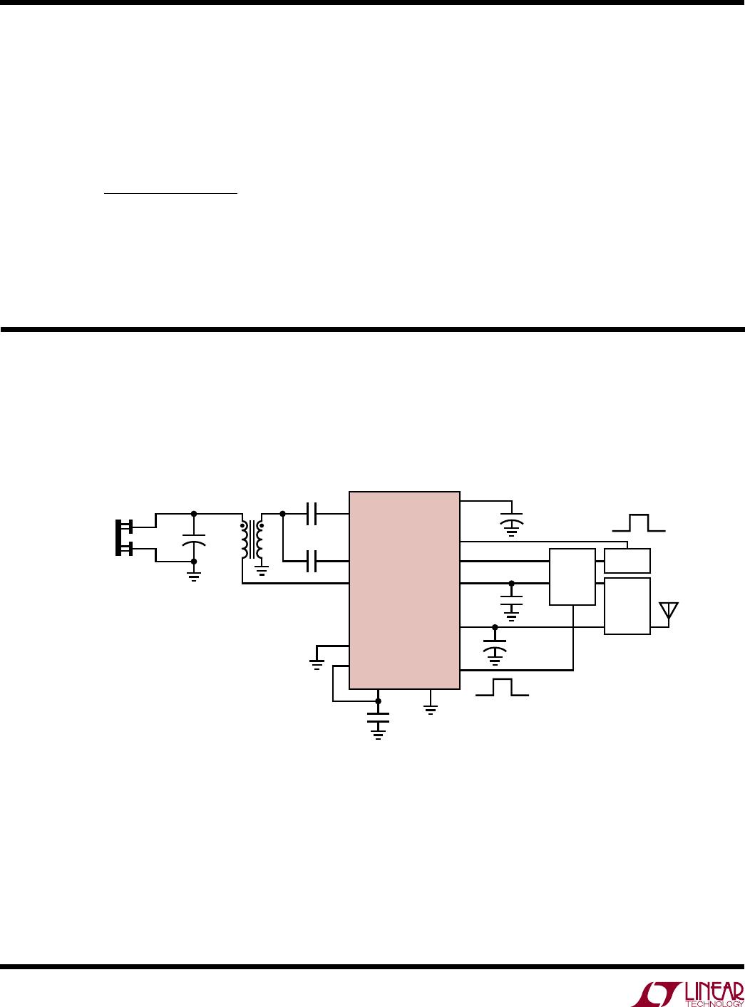
Design Example 2
In many pulsed load applications, the duration, magnitude
and frequency of the load current bursts are known and
fixed. In these cases, the average charge current required
from the LTC3108 to support the average load must be
calculated, which can be easily done by the following:
≥+II
CHGQ
BURST
Where I
Q
is the sleep current on V
OUT
required by the ex-
ternal circuitry in between bursts (including cap leakage),
I
BURST
is the total load current during the burst, t is the