LTC3108
7
3108fc
For more information www.linear.com/LTC3108
VAUX (Pin 1/Pin 2): Output of the Internal Rectifier Cir-
cuit and V
CC
for the IC. Bypass VAUX with at least 1µF of
capacitance. An active shunt regulator clamps VAUX to
5.25V (typical).
VSTORE (Pin 2/Pin 3): Output for the Storage Capacitor
or Battery. A large capacitor may be connected from this
pin to GND for powering the system in the event the input
voltage is lost. It will be charged up to the maximum VAUX
clamp voltage. If not used, this pin should be left open
or tied to VAUX.
V
OUT
(Pin 3/Pin 4): Main Output of the Converter. The
voltage at this pin is regulated to the voltage selected by
VS1 and VS2 (see Table 1). Connect this pin to an energy
storage capacitor or to a rechargeable battery.
V
OUT2
(Pin 4/Pin 5): Switched Output of the Converter.
Connect this pin to a switched load. This output is open
until V
OUT2_EN
is driven high, then it is connected to
V
OUT
through a 1.3Ω P-channel switch. If not used, this
pin should be left open or tied to V
OUT
. The peak current
in this output is limited to 0.3A typical.
VLDO (Pin 5/Pin 6): Output of the 2.2V LDO. Connect a
2.2µF or larger ceramic capacitor from this pin to GND.
If not used, this pin should be tied to VAUX.
PGD (Pin 6/Pin 7): Power Good Output. When V
OUT
is
within 7.5% of its programmed value, PGD will be pulled
up to VLDO through a 1MΩ resistor. If V
OUT
drops 9%
below its programmed value PGD will go low. This pin
can sink up to 100µA.
VS2 (Pin 7/Pin 10): V
OUT
Select Pin 2. Connect this pin
to ground or VAUX to program the output voltage (see
Table 1).
VS1 (Pin 8/Pin 11): V
OUT
Select Pin 1. Connect this pin
to ground or VAUX to program the output voltage (see
Table 1).
V
OUT2_EN
(Pin 9/Pin 12): Enable Input for V
OUT2
. V
OUT2
will be enabled when this pin is driven high. There is an
internal 5M pull-down resistor on this pin. If not used,
this pin can be left open or grounded.
C1 (Pin 10/Pin 13): Input to the Charge Pump and Rectifier
Circuit. Connect a capacitor from this pin to the secondary
winding of the step-up transformer.
C2 (Pin 11/Pin 14): Input to the N-Channel Gate Drive
Circuit. Connect a capacitor from this pin to the secondary
winding of the step-up transformer.
SW (Pin 12/Pin 15): Drain of the Internal N-Channel
Switch. Connect this pin to the primary winding of the
transformer.
GND (Pins 1, 8, 9, 16) SSOP Only: Ground
GND (Exposed Pad Pin 13) DFN Only: Ground. The DFN
exposed pad must be soldered to the PCB ground plane.
It serves as the ground connection, and as a means of
conducting heat away from the die.
Table 1. Regulated Voltage Using Pins VS1 and VS2
VS2 VS1 V
OUT
GND GND 2.35V
GND VAUX 3.3V
VAUX GND 4.1V
VAUX VAUX 5V
pin FuncTions
(DFN/SSOP)
LTC3108
8
3108fc
For more information www.linear.com/LTC3108
block DiagraM
operaTion
The LTC3108 is designed to use a small external step-up
transformer to create an ultralow input voltage step-up
DC/DC converter and power manager. It is ideally suited
for low power wireless sensors and other applications in
which surplus energy harvesting is used to generate system
power because traditional battery power is inconvenient
or impractical.
The LTC3108 is designed to manage the charging and
regulation of multiple outputs in a system in which the
average power draw is very low, but there may be periodic
pulses of higher load current required. This is typical of
wireless sensor applications, where the quiescent power
draw is extremely low most of the time, except for transmit
bursts when circuitry is powered up to make measure
-
ments and transmit data.
The LTC3108 can also be used to trickle charge a standard
capacitor, supercapacitor or rechargeable battery, using
energy harvested from a Peltier or photovoltaic cell.
(Refer to the Block Diagram)
3108 BD
C1
C2
5M
SW
5.25V
1.2V
V
REF
SW
V
OUT
VSTORE
VLDO
OFF ON
V
OUT2
V
OUT2
V
OUT
V
OUT
PROGRAM
C
OUT
PGOOD
V
OUT2_EN
V
OUT
VS1
VS2
PGD
VSTORE
C1
C
IN
V
IN
VLDO
C
STORE
F
1:100
C2
SYNC RECTIFY REFERENCE
V
OUT
2.2V
CHARGE
CONTROL
VAUX
+
+
ILIM
LTC3108
1.3Ω
0.5Ω
1M
EXPOSED PAD (DFN)
2.2µF
GND (SSOP)
V
REF
LDO
V
REF
V
BEST
LTC3108
9
3108fc
For more information www.linear.com/LTC3108
operaTion
Oscillator
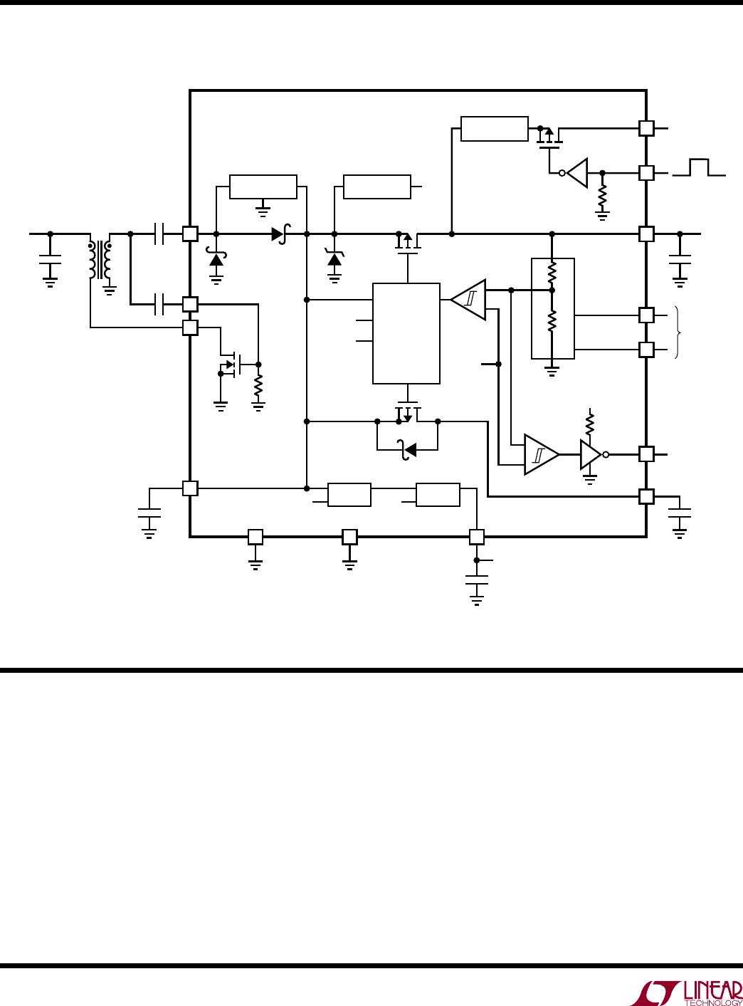
The LTC3108 utilizes a MOSFET switch to form a resonant
step-up oscillator using an external step-up transformer
and a small coupling capacitor. This allows it to boost input
voltages as low as 20mV high enough to provide multiple
regulated output voltages for powering other circuits. The
frequency of oscillation is determined by the inductance of
the transformer secondary winding and is typically in the
range of 10kHz to 100kHz. For input voltages as low as
20mV, a primary-secondary turns ratio of about 1:100 is
recommended. For higher input voltages, this ratio can be
lower. See the Applications Information section for more
information on selecting the transformer.
Charge Pump and Rectifier
The AC voltage produced on the secondary winding of
the transformer is boosted and rectified using an external
charge pump capacitor (from the secondary winding to pin
C1) and the rectifiers internal to the LTC3108. The rectifier
circuit feeds current into the VAUX pin, providing charge
to the external VAUX capacitor and the other outputs.
VAUX
The active circuits within the LTC3108 are powered from
VAUX, which should be bypassed with a 1µF capacitor.
Larger capacitor values are recommended when using
turns ratios of 1:50 or 1:20 (refer to the Typical Applica
-
tion examples). Once VAUX exceeds 2.5V, the main V
OUT
is allowed to start charging.
An internal shunt regulator limits the maximum voltage
on VAUX to 5.25V typical. It shunts to GND any excess
current into VAUX when there is no load on the converter
or the input source is generating more power than is
required by the load.
Voltage Reference
The LTC3108 includes a precision, micropower reference,
for accurate regulated output voltages. This reference
becomes active as soon as VAUX exceeds 2V.
Synchronous Rectifiers
Once VAUX exceeds 2V, synchronous rectifiers in parallel
with each of the internal diodes take over the job of rectify
-
ing the input voltage, improving efficiency.
Low Dropout Linear Regulator (LDO)
The LTC3108 includes a low current LDO to provide a
regulated 2.2V output for powering low power proces
-
sors or other low power ICs. The LDO is powered by the
higher of VAUX or V
OUT
. This enables it to become active
as soon as VAUX has charged to 2.3V, while the V
OUT
stor-
age capacitor is still charging. In the event of a step load
on the LDO output, current can come from the main V
OUT
capacitor if VAUX drops below V
OUT
. The LDO requires
a 2.2µF ceramic capacitor for stability. Larger capacitor
values can be used without limitation, but will increase
the time it takes for all the outputs to charge up. The LDO
output is current limited to 4mA minimum.
V
OUT
The main output voltage on V
OUT
is charged from the VAUX
supply, and is user programmed to one of four regulated
voltages using the voltage select pins VS1 and VS2, ac
-
cording to Table 2. Although the logic threshold voltage
for VS1 and VS2 is 0.85V typical, it is recommended that
they be tied to ground or VAUX.
Table 2. Regulated Voltage Using Pins VS1 and VS2
VS2 VS1 V
OUT
GND GND 2.35V
GND VAUX 3.3V
VAUX GND 4.1V
VAUX VAUX 5V
When the output voltage drops slightly below the regulated
value, the charging current will be enabled as long as VAUX
is greater than 2.5V. Once V
OUT
has reached the proper
value, the charging current is turned off.
The internal programmable resistor divider sets V
OUT
,
eliminating the need for very high value external resistors
that are susceptible to board leakage.

LTC3108EDE#PBF

Mfr. #:
Manufacturer:
Analog Devices / Linear Technology
Description:
Switching Voltage Regulators Ultralow Voltage Step-Up Converter and Power Manager
Lifecycle:
New from this manufacturer.
Delivery:
DHL FedEx Ups TNT EMS
Payment:
T/T Paypal Visa MoneyGram Western Union