1.35V DDR3L SDRAM UDIMM
MT8KTF12864AZ – 1GB
MT8KTF25664AZ – 2GB
MT8KTF51264AZ – 4GB
Features
DDR3L functionality and operations supported as
defined in the component data sheet
240-pin, unbuffered dual in-line memory module
(UDIMM)
Fast data transfer rates: PC3-14900, PC3-12800, or
PC3-10600
1GB (128 Meg x 64), 2GB (256 Meg x 64), or 4GB (512
Meg x 64)
V
DD
= V
DDQ
= 1.35V (1.238–1.45V)
V
DD
= V
DDQ
= 1.5V (1.425–1.575V)
Backward-compatible to V
DD
= V
DDQ
= 1.5V ±0.075V
V
DDSPD
= 3.0–3.6V
Reset pin for improved system stability
Nominal and dynamic on-die termination (ODT) for
data, strobe, and mask signals
Single-rank
Fixed burst chop (BC) of 4 and burst length (BL) of 8
via the mode register set (MRS)
Adjustable data-output drive strength
Serial presence-detect (SPD) EEPROM
Gold edge contacts
Halogen-free
Fly-by topology
Terminated control, command, and address bus
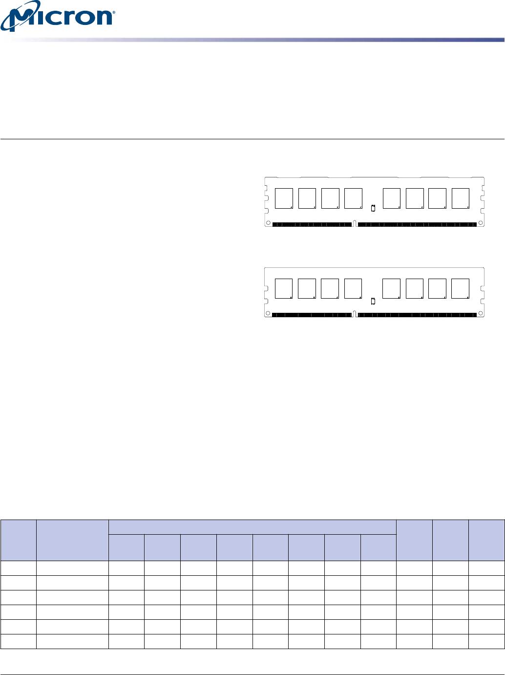
Figure 1: 240-Pin UDIMM (MO-269 R/C-A)
Module height: 30mm (1.181in)
Figure 2: 240-Pin UDIMM (MO-269 R/C-A1)
Module Height: 30.0mm (1.181in)
Options
Marking
Operating temperature
Commercial (0°C T
A
70°C) None
Package
240-pin DIMM (halogen-free) Z
Frequency/CAS latency
1.07ns @ CL = 13 (DDR3-1866) -1G9
1.25ns @ CL = 11 (DDR3-1600) -1G6
1.5ns @ CL = 9 (DDR3-1333) -1G4
Table 1: Key Timing Parameters
Speed
Grade
Industry
Nomenclature
Data Rate (MT/s)
t
RCD
(ns)
t
RP
(ns)
t
RC
(ns)
CL =
13
CL =
11
CL =
10 CL = 9 CL = 8 CL = 7 CL = 6 CL = 5
-1G9 PC3-14900 1866 1600 1333 1333 1066 1066 800 667 13.125 13.125 47.125
-1G6 PC3-12800 1600 1333 1333 1066 1066 800 667 13.125 13.125 48.125
-1G4 PC3-10600 1333 1333 1066 1066 800 667 13.125 13.125 49.125
-1G1 PC3-8500 1066 1066 800 667 13.125 13.125 50.625
-1G0 PC3-8500 1066 800 667 15 15 52.5
-80B PC3-6400 800 667 15 15 52.5
1GB, 2GB, 4GB (x64, SR) 240-Pin 1.35V DDR3L UDIMM
Features
PDF: 09005aef8413b5fe
ktf8c128_256_512x64az.pdf – Rev. K 9/15 EN
1
Micron Technology, Inc. reserves the right to change products or specifications without notice.
© 2010 Micron Technology, Inc. All rights reserved.
Products and specifications discussed herein are subject to change by Micron without notice.
Table 2: Addressing
Parameter 1GB 2GB 4GB
Refresh count 8K 8K 8K
Row address 16K A[13:0] 32K A[14:0] 64K A[15:0]
Device bank address 8 BA[2:0] 8 BA[2:0] 8 BA[2:0]
Device configuration 1Gb (128 Meg x 8) 2Gb (256 Meg x 8) 4Gb (512 Meg x 8)
Column address 1K A[9:0] 1K A[9:0] 1K A[9:0]
Module rank address 1 S0# 1 S0# 1 S0#
Table 3: Part Numbers and Timing Parameters – 1GB Modules
Base device: MT41K128M8,
1
1Gb DDR3L SDRAM
Part Number
2
Module
Density Configuration
Module
Bandwidth
Memory Clock/
Data Rate
Clock Cycles
(CL-
t
RCD-
t
RP)
MT8KTF12864AZ-1G6__ 1GB 128 Meg x 64 12.8 GB/s 1.25ns/1600 MT/s 11-11-11
MT8KTF12864AZ-1G4__ 1GB 128 Meg x 64 10.6 GB/s 1.5ns/1333 MT/s 9-9-9
Table 4: Part Numbers and Timing Parameters – 2GB Modules
Base device: MT41K256M8,
1
2Gb DDR3L SDRAM
Part Number
2
Module
Density Configuration
Module
Bandwidth
Memory Clock/
Data Rate
Clock Cycles
(CL-
t
RCD-
t
RP)
MT8KTF25664AZ-1G6__ 2GB 256 Meg x 64 12.8 GB/s 1.25ns/1600 MT/s 11-11-11
MT8KTF25664AZ-1G4__ 2GB 256 Meg x 64 10.6 GB/s 1.5ns/1333 MT/s 9-9-9
Table 5: Part Numbers and Timing Parameters – 4GB Modules
Base device: MT41K512M8,
1
4Gb DDR3L SDRAM
Part Number
2
Module
Density Configuration
Module
Bandwidth
Memory Clock/
Data Rate
Clock Cycles
(CL-
t
RCD-
t
RP)
MT8KTF51264AZ-1G9__ 4GB 512 Meg x 64 14.9 GB/s 1.07ns/1866 MT/s 13-13-13
MT8KTF51264AZ-1G6__ 4GB 512 Meg x 64 12.8 GB/s 1.25ns/1600 MT/s 11-11-11
Notes:
1. Data sheets for the base device parts can be found on Micron’s Web site.
2. All part numbers end with a two-place code (not shown) that designates component and PCB revisions.
Consult factory for current revision codes. Example: MT8KTF51264AZ-1G9P1.
1GB, 2GB, 4GB (x64, SR) 240-Pin 1.35V DDR3L UDIMM
Features
PDF: 09005aef8413b5fe
ktf8c128_256_512x64az.pdf – Rev. K 9/15 EN
2
Micron Technology, Inc. reserves the right to change products or specifications without notice.
© 2010 Micron Technology, Inc. All rights reserved.
Pin Assignments
Table 6: Pin Assignments
240-Pin DDR3 UDIMM Front 240-Pin DDR3 UDIMM Back
Pin Symbol Pin Symbol Pin Symbol Pin Symbol Pin Symbol Pin Symbol Pin Symbol Pin Symbol
1 V
REFDQ
31 DQ25 61 A2 91 DQ41 121 V
SS
151 V
SS
181 A1 211 V
SS
2 V
SS
32 V
SS
62 V
DD
92 V
SS
122 DQ4 152 DM3 182 V
DD
212 DM5
3 DQ0 33 DQS3# 63 NF 93 DQS5# 123 DQ5 153 NC 183 V
DD
213 NC
4 DQ1 34 DQS3 64 NF 94 DQS5 124 V
SS
154 V
SS
184 CK0 214 V
SS
5 V
SS
35 V
SS
65 V
DD
95 V
SS
125 DM0 155 DQ30 185 CK0# 215 DQ46
6 DQS0# 36 DQ26 66 V
DD
96 DQ42 126 NC 156 DQ31 186 V
DD
216 DQ47
7 DQS0 37 DQ27 67 V
REFCA
97 DQ43 127 V
SS
157 V
SS
187 NC 217 V
SS
8 V
SS
38 V
SS
68 NC 98 V
SS
128 DQ6 158 NC 188 A0 218 DQ52
9 DQ2 39 NC 69 V
DD
99 DQ48 129 DQ7 159 NC 189 V
DD
219 DQ53
10 DQ3 40 NC 70 A10 100 DQ49 130 V
SS
160 V
SS
190 BA1 220 V
SS
11 V
SS
41 V
SS
71 BA0 101 V
SS
131 DQ12 161 NC 191 V
DD
221 DM6
12 DQ8 42 NC 72 V
DD
102 DQS6# 132 DQ13 162 NC 192 RAS# 222 NC
13 DQ9 43 NC 73 WE# 103 DQS6 133 V
SS
163 V
SS
193 S0# 223 V
SS
14 V
SS
44 V
SS
74 CAS# 104 V
SS
134 DM1 164 NC 194 V
DD
224 DQ54
15 DQS1# 45 NC 75 V
DD
105 DQ50 135 NC 165 NC 195 ODT0 225 DQ55
16 DQS1 46 NC 76 NC 106 DQ51 136 V
SS
166 V
SS
196 A13 226 V
SS
17 V
SS
47 V
SS
77 NC 107 V
SS
137 DQ14 167 NC 197 V
DD
227 DQ60
18 DQ10 48 NC 78 V
DD
108 DQ56 138 DQ15 168 RESET# 198 NC 228 DQ61
19 DQ11 49 NC 79 NC 109 DQ57 139 V
SS
169 NC 199 V
SS
229 V
SS
20 V
SS
50 CKE0 80 V
SS
110 V
SS
140 DQ20 170 V
DD
200 DQ36 230 DM7
21 DQ16 51 V
DD
81 DQ32 111 DQS7# 141 DQ21 171 NF/A15
1
201 DQ37 231 NC
22 DQ17 52 BA2 82 DQ33 112 DQS7 142 V
SS
172 NF/A14
2
202 V
SS
232 V
SS
23 V
SS
53 NC 83 V
SS
113 V
SS
143 DM2 173 V
DD
203 DM4 233 DQ62
24 DQS2# 54 V
DD
84 DQS4# 114 DQ58 144 NC 174 A12 204 NC 234 DQ63
25 DQS2 55 A11 85 DQS4 115 DQ59 145 V
SS
175 A9 205 V
SS
235 V
SS
26 V
SS
56 A7 86 V
SS
116 V
SS
146 DQ22 176 V
DD
206 DQ38 236 V
DDSPD
27 DQ18 57 V
DD
87 DQ34 117 SA0 147 DQ23 177 A8 207 DQ39 237 SA1
28 DQ19 58 A5 88 DQ35 118 SCL 148 V
SS
178 A6 208 V
SS
238 SDA
29 V
SS
59 A4 89 V
SS
119 SA2 149 DQ28 179 V
DD
209 DQ44 239 V
SS
30 DQ24 60 V
DD
90 DQ40 120 V
TT
150 DQ29 180 A3 210 DQ45 240 V
TT
Notes:
1. Pin 171 is NF for 1GB and 2GB; A14 for 4GB.
2. Pin 172 is NF for 1GB; A14 for 2GB and 4GB.
1GB, 2GB, 4GB (x64, SR) 240-Pin 1.35V DDR3L UDIMM
Pin Assignments
PDF: 09005aef8413b5fe
ktf8c128_256_512x64az.pdf – Rev. K 9/15 EN
3
Micron Technology, Inc. reserves the right to change products or specifications without notice.
© 2010 Micron Technology, Inc. All rights reserved.

MT8KTF51264AZ-1G9P1

Mfr. #:
Manufacturer:
Micron
Description:
Memory Modules DDR3 4GB UDIMM
Lifecycle:
New from this manufacturer.
Delivery:
DHL FedEx Ups TNT EMS
Payment:
T/T Paypal Visa MoneyGram Western Union