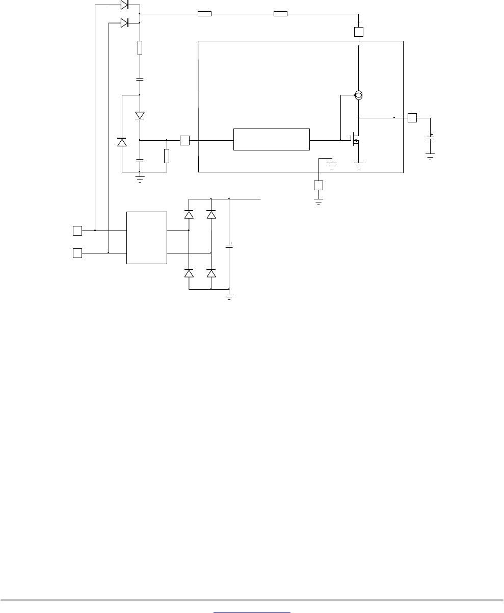
NCP1339
www.onsemi.com
21
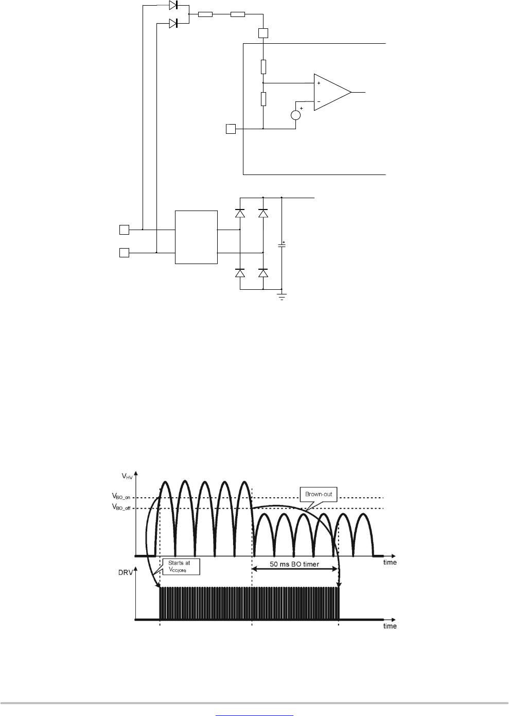
Figure 49. Simplified Block Diagram of the Remote Control Input
V_REM_off
Vcc
C2
GND
REM to Vcc
management
R2
R1
C3
D2
D1
C1
REM
In summary, the REM pin works as follows:
• When pulled below a certain level (V_REM_on, 1.5 V
typical), the power supply operates normally. As
capacitors are connected to this pin, it is important to
discharge them properly during the start−up sequence.
A 100−ms timer performs this function by pulling the
pin to ground. It is operating in any re−start conditions
(brown−out recovery, short−circuit, latch reset and so
on) except in the self−relaxing PSM mode ( during
which the voltage on the pin swings up and down.
• When brought above a certain level (V_REM_off, 8 V
typical), the power supply stops working. In the
absence of an external bias, the remote pin starts to
drop at a pace imposed by the various time constants
around it. During this mode, despite the absence of V
cc
,
the X2 discharge circuitry remains active and monitors
the ac input line.
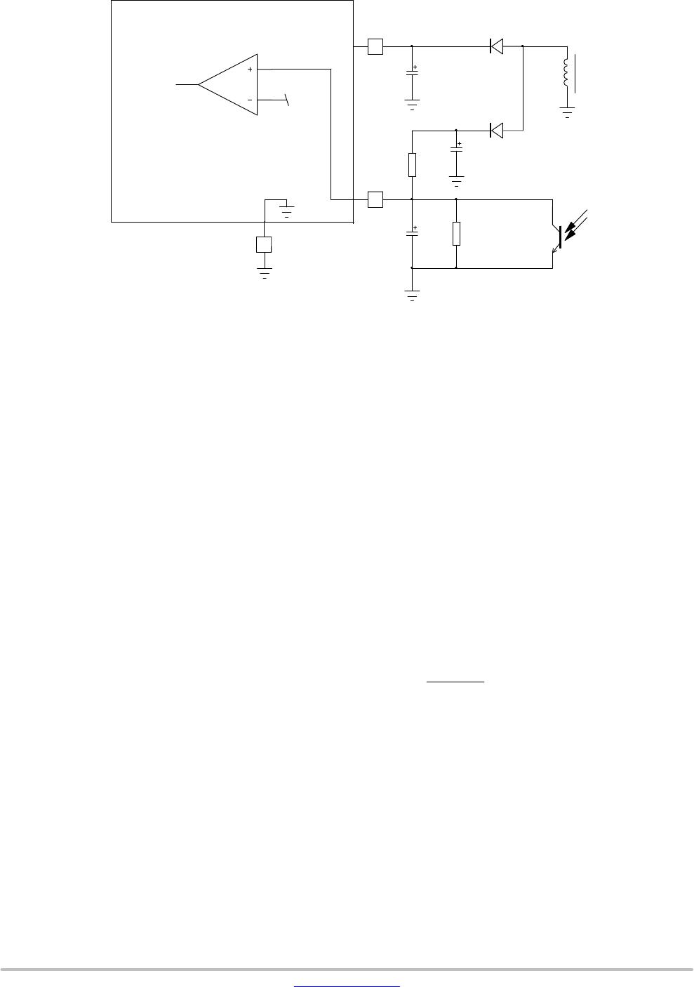
Fault Input
The NCP1339 includes a dedicated fault input accessible
via the Fault pin. Figure 50 shows the architecture of the
Fault input. The controller can be latched by pulling up the
pin above the upper fault threshold, V
Fault(OVP)
, typically
3.0 V. An active clamp prevents the Fault pin voltage from
reaching the V
Fault(OVP)
if the pin is open. To reach the upper
threshold, the external pull−up current has to be higher than
the pull−down capability of the clamp (set by R
Fault(clamp)
at
V
Fault(clamp)
), i.e., approximately 1 mA.
This function is typically used to detect a V
CC
or auxiliary
winding overvoltage by means of a Zener diode generally in
series with a small resistor (see Figure 50).
Neglecting the resistor voltage drop, the OVP threshold is
then:
V
AUX(OVP)
+ V
Z
) V
Fault(OVP)
,
(eq. 4)
where VZ is the Zener diode voltage.
The controller can also be latched off if the Fault pin
voltage, V
Fault
, is pulled below the lower fault threshold,
V
Fault(OTP_in)
, typically 0.4 V. This capability is normally
used for detecting an overtemperature fault by means of an
NTC thermistor. A pull up current source I
Fault(OTP)
,
(typically 45.5 mA) generates a voltage drop across the
thermistor. The resistance of the NTC thermistor decreases
at higher temperatures resulting in a lower voltage across the
thermistor. The controller detects a fault once the thermistor
voltage drops below V
Fault(OTP_in)
.
The circuit detects an overtemperature situation when:
R
NTC
@ I
Fault(OTP)
+ V
Fault(OTP)
.
(eq. 5)
Hence, the OTP protection trips when
R
NTC
+
V
Fault(OTP)
I
Fault(OTP)
(eq. 6)
that is 8.8 kohms typically.
The controller bias current is reduced during power up by
disabling most of the circuit blocks including I
Fault(OTP)
.
This current source is enabled once V
CC
reaches V
CC(on)
. A
bypass capacitor is usually connected between the Fault and
GND pins. It will take some time for V
Fault
to reach its steady
state value once I
Fault(OTP)
is enabled. Therefore, the lower
fault comparator (i.e. overtemperature detection) is ignored
during soft−start.