GTL2014 All information provided in this document is subject to legal disclaimers. © NXP B.V. 2012. All rights reserved.
Product data sheet Rev. 3 — 14 June 2012 5 of 19
NXP Semiconductors
GTL2014
4-bit LVTTL to GTL transceiver
7. Functional description
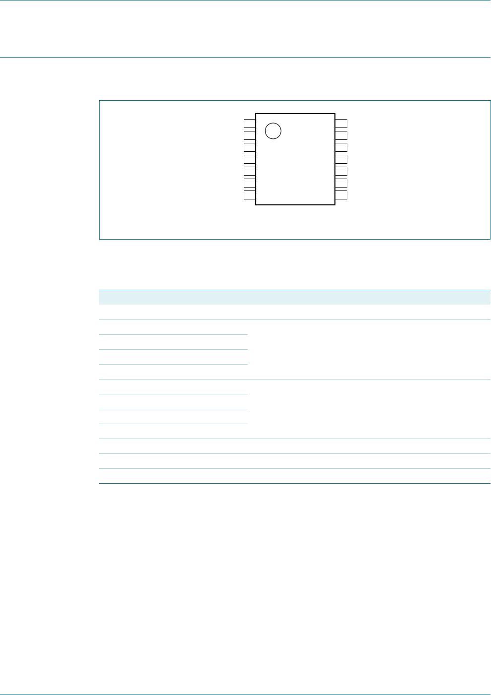
Refer to Figure 2 “Logic diagram for GTL2014”.
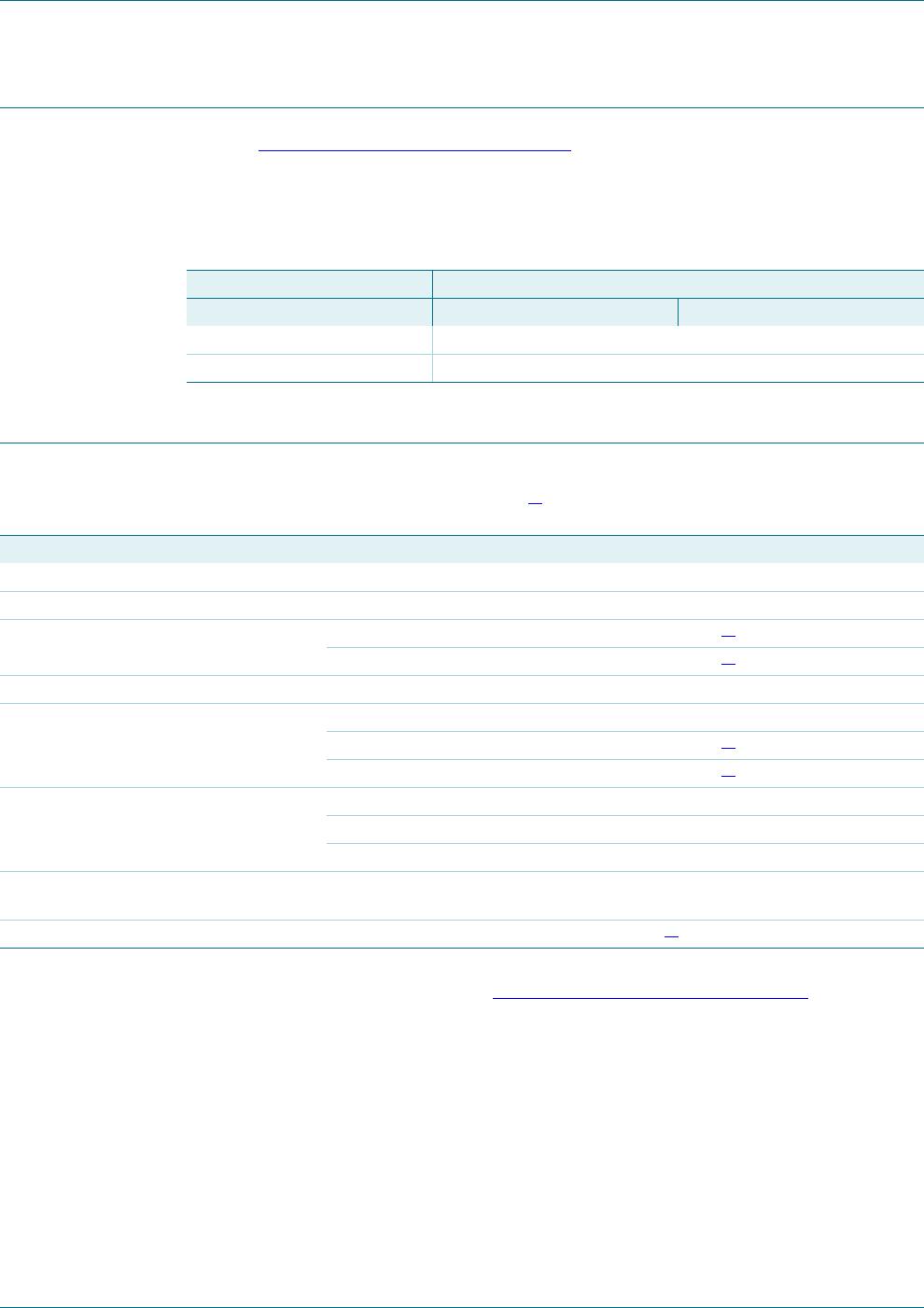
7.1 Function table
8. Limiting values
[1] Stresses beyond those listed may cause permanent damage to the device. These are stress ratings only and functional operation of the
device at these or any other conditions beyond those indicated under Section 9 “
Recommended operating conditions” is not implied.
Exposure to absolute-maximum-rated conditions for extended periods may affect device reliability.
[2] The input and output negative voltage ratings may be exceeded if the input and output clamp current ratings are observed.
[3] The performance capability of a high-performance integrated circuit in conjunction with its thermal environment can create junction
temperatures which are detrimental to reliability. The maximum junction temperature of this integrated circuit should not exceed 150 °C.
Table 5. Function table
H = HIGH voltage level; L = LOW voltage level.
Input Input/output
DIR A (LVTTL) B (GTL)
H input Bn = An
L An = Bn input
Table 6. Limiting values
In accordance with the Absolute Maximum Rating System (IEC 60134).
[1]
Voltages are referenced to GND (ground = 0 V).
Symbol Parameter Conditions Min Max Unit
V
CC
supply voltage −0.5 +4.6 V
I
IK
input clamping current V
I
<0V - −50 mA
V
I
input voltage A port −0.5
[2]
+7.0 V
B port −0.5
[2]
+4.6 V
I
OK
output clamping current A port; V
O
<0V - −50 mA
V
O
output voltage output in OFF or HIGH state
A port −0.5
[2]
+7.0 V
B port −0.5
[2]
+4.6 V
I
OL
LOW-level output current current into any output in the LOW state
A port - 32 mA
B port - 80 mA
I
OH
HIGH-level output current current into any output in the HIGH state;
A port
- −32 mA
T
stg
storage temperature
[3]
−60 +150 °C