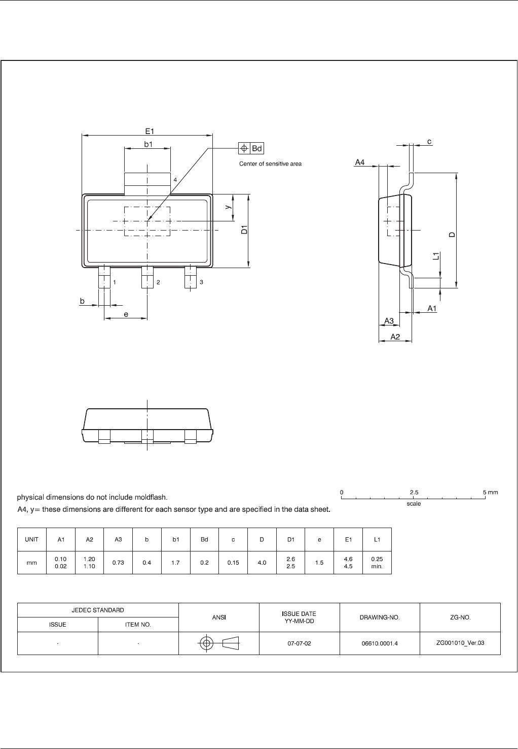
HAL 1820 DATA SHEET
10 July 3, 2013; DSH000158_003EN Micronas
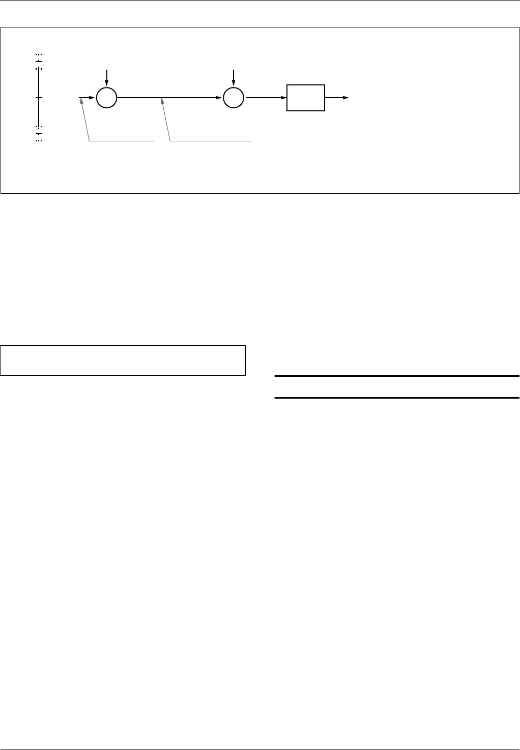
Fig. 2–3: Signal path HAL1820
2.2.4. Signal Path
Fig. 2–3 shows the signal path and signal processing
of HAL1820. The measurement output value y is cal-
culated out of the input signal X with the following
equation
The parameters offset and sensitivity are two’s com-
plement encoded 8-bit values (see Section 2.2.1. on
page 8).
2.3. Calibration Procedure
2.3.1. General Procedure
For calibration in the system environment, the applica-
tion kit from Micronas is recommended. It contains the
hardware for the generation of the serial telegram for
programming and the corresponding software for the
input of the register values.
For the individual calibration of each sensor in the cus-
tomer application, a two-point adjustment is recom-
mended. Please use Micronas Software Kit for the cal-
ibration.
Locking the Sensor
The last step is activating the LOCK function by setting
the LOCK bit. Please note that the LOCK function
becomes effective after power-down and power-up of
the Hall IC. The sensors EEPROM is then locked and
its content can not be changed anymore. The sensor
still answers to read commands on the supply line.
Warning: This register cannot be reset!
y
ADC
+FS
FS
FS range
~
~
}
±1
+
±0.5 (OALN = 0)
±0.125 (OALN = 1)
8-bit offset value (128...+127)
*
±2
8-bit sensitivity value (128...+127)
10-bit readout-value (512...+511)
±1 @ offset = 0 and sensitivity = 1
Definition: FS of ADC = 1.
0
{
{
clamp
y/n
ADC value
adder out
range ±7936
range 8192/8191
range
+range
Y sensitivity X OFFSET–=