HAL 1820 DATA SHEET
22 July 3, 2013; DSH000158_003EN Micronas
4. Application Notes
4.1. Ambient Temperature
Due to the internal power dissipation, the temperature
on the silicon chip (junction temperature T
J
) is higher
than the temperature outside the package (ambient
temperature T
A
).
T
J
= T
A
+ T
At static conditions and continuous operation, the fol-
lowing equation applies:
T = I
SUP
* V
SUP
* R
thjX
The X represents junction to air or to case.
For worst case calculation, use the max. parameters
for I
SUP
and R
thjX
, and the max. value for V
SUP
from
the application.
The following example shows the result for junction to
air conditions. V
SUP
= 5.5 V, R
thja
= 250 K/W and I
SUP
= 10 mA the temperature difference T = 13.75 K.
The junction temperature T
J
is specified. The maxi-
mum ambient temperature T
Amax
can be calculated as:
T
Amax
= T
Jmax
T
4.2. EMC and ESD
The HAL1820 is designed for a stabilized 5 V supply.
Interferences and disturbances conducted along the
12 V onboard system (product standard ISO 7637 part
1) are not relevant for these applications.
For applications with disturbances by capacitive or
inductive coupling on the supply line or radiated distur-
bances, the application circuit shown in Fig. 4–1 is rec-
ommended. Applications with this arrangement should
pass the EMC tests according to the product stan-
dards ISO 7637 part 3 (Electrical transient transmis-
sion by capacitive or inductive coupling) and part 4
(Radiated disturbances).
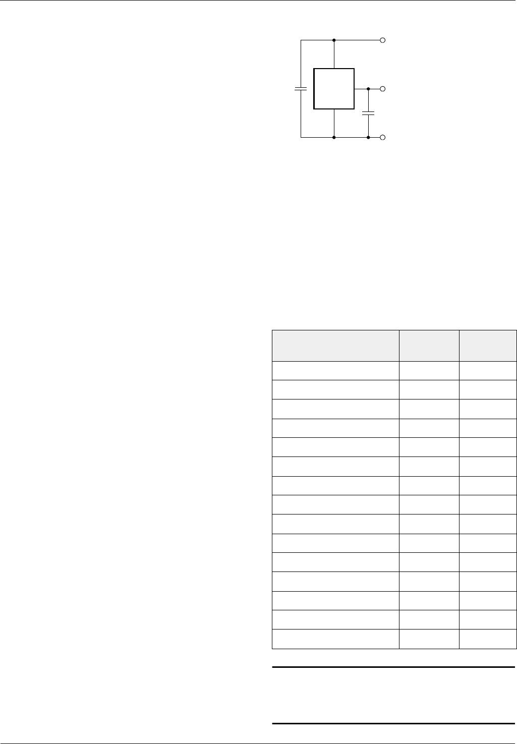
4.3. Application Circuit
For EMC protection, it is recommended to connect one
ceramic 47 nF capacitor between ground and output
voltage pin as well as 100 nF between supply and
ground.
Fig. 4–1: Recommended application circuit
4.4. Temperature Compensation
The relationship between the temperature coefficient
of the magnet and the corresponding TC and TCSQ
codes for linear compensation is given in the following
table. In addition to the linear change of the magnetic
field with temperature, the curvature can be adjusted
as well. For this purpose, other TC and TCSQ combi-
nations are required which are not shown in the table.
Please contact Micronas for more detailed information
on this higher order temperature compensation.
Note: Micronas recommends to use the HAL1820
Programming Environment to find optimal set-
tings for temperature coefficients. Please con-
tact Micronas for more detailed information.
Temperature Coefficient
of Magnet (ppm/K)
TC TCSQ
2100 8 0
1800 10 3
1500 12 4
1200 14 5
900 16 6
500 18 6
150 20 6
0215
300 22 5
500 23 4
750 24 4
1000 25 2
1500 27 0
2100 29 5
2700 31 5
OUT
V
SUP
GND
100 nF
HAL1820
47 nF
DATA SHEET HAL 1820
Micronas July 3, 2013; DSH000158_003EN 23
5. Programming of the Sensor
HAL1820 features two different customer modes. In
Application Mode the sensor provides a ratiometric
analog output voltage. In Programming Mode it is
possible to change the register settings of the sensor.
After power-up the sensor is always operating in the
Programming Mode (default after delivery from
Micronas and as long as the sensor is not locked). It is
switched to the Application Mode by setting a certain
volatile bit in the memory of the sensor or by locking
the sensor.
5.1. Programming Interface
In Programming Mode the sensor is addressed by
modulating a serial telegram on the sensors supply
voltage. The sensor answers with a modulation of the
output voltage.
A logical “0” is coded as no level change within the bit
time. A logical “1” is coded as a level change of typi-
cally 50% of the bit time. After each bit, a level change
occurs (see Fig. 5–1).
The serial telegram is used to transmit the EEPROM
content, error codes and digital values of the magnetic
field from and to the sensor.
Fig. 5–1: Definition of logical 0 and 1 bit
A description of the communication protocol and the
programming of the sensor is available in a separate
document (Application Note Programming HAL1820).
t
r
t
f
t
p0
t
p0
logical 0
V
DDH
V
DDL
or
t
p0
logical 1
V
DDH
V
DDL
or
t
p0
t
p1
t
p1
Table 5–1: Telegram parameters (All voltages are referenced to GND.)
Symbol Parameter Pin No. Limit Values Unit Test Conditions
Min. Typ. Max.
V
SUPL
Supply Voltage for Low Level
during Programming through
Sensor V
SUP
Pin
1 5.8 6.3 6.6 V
V
SUPH
Supply Voltage for High Level
during Programming through
Sensor V
SUP
Pin
1 6.8 7.3 7.8 V
V
SUPProgram
V
SUP
Voltage for EEPROM
programming (after PROG and
ERASE)
1 5.7 5.85 6.0 V
t
p0
Bit time if command send to the
sensor
1 1024 µs
t
pOUT
Bit time for sensor answer 3 1024 µs
HAL 1820 DATA SHEET
24 July 3, 2013; DSH000158_003EN Micronas
5.2. Programming Environment and Tools
For the programming of HAL1820 during product
development and also for production purposes a pro-
gramming tool including hardware and software is
available on request. It is recommended to use the
Micronas tool kit in order to easy the product develop-
ment. The details of programming sequences are also
available on request.
5.3. Programming Information
For production and qualification tests, it is mandatory
to set the LOCK bit after final adjustment and program-
ming of HAL1820. The LOCK function is active after
the next power-up of the sensor.
The success of the LOCK process should be checked
by reading the status of the LOCK bit after locking and/
or by an analog check of the sensors output signal.
HAL1820 features a diagnostic register to check the
success and quality of the programming process. It is
mandatory to check that all bits of the DIAGN register
are 0 after the programming of the sensor. More
details can be found in the application note “HAL1820
Programming Guide”.
Electrostatic Discharges (ESD) may disturb the pro-
gramming pulses. Please take precautions against
ESD.

HAL1820SF-A

Mfr. #:
Manufacturer:
TDK-Micronas
Description:
Board Mount Hall Effect / Magnetic Sensors Programmable Linear Hall Sensor
Lifecycle:
New from this manufacturer.
Delivery:
DHL FedEx Ups TNT EMS
Payment:
T/T Paypal Visa MoneyGram Western Union

Products related to this Datasheet