REV. D
a
AD8001
Information furnished by Analog Devices is believed to be accurate and
reliable. However, no responsibility is assumed by Analog Devices for its
use, nor for any infringements of patents or other rights of third parties that
may result from its use. No license is granted by implication or otherwise
under any patent or patent rights of Analog Devices. Trademarks and
registered trademarks are the property of their respective companies.
One Technology Way, P.O. Box 9106, Norwood, MA 02062-9106, U.S.A.
Tel: 781/329-4700 www.analog.com
Fax: 781/326-8703 © 2003 Analog Devices, Inc. All rights reserved.
800 MHz, 50 mW
Current Feedback Amplifier
FEATURES
Excellent Video Specifications (R
L
= 150 , G = +2)
Gain Flatness 0.1 dB to 100 MHz
0.01% Differential Gain Error
0.025 Differential Phase Error
Low Power
5.5 mA Max Power Supply Current (55 mW)
High Speed and Fast Settling
880 MHz, –3 dB Bandwidth (G = +1)
440 MHz, –3 dB Bandwidth (G = +2)
1200 V/s Slew Rate
10 ns Settling Time to 0.1%
Low Distortion
–65 dBc THD, f
C
= 5 MHz
33 dBm Third Order Intercept, F
1
= 10 MHz
–66 dB SFDR, f = 5 MHz
High Output Drive
70 mA Output Current
Drives Up to 4 Back-Terminated Loads (75 Each)
While Maintaining Good Differential Gain/Phase
Performance (0.05%/0.25)
APPLICATIONS
A-to-D Drivers
Video Line Drivers
Professional Cameras
Video Switchers
Special Effects
RF Receivers
1
2
3
4
8
7
6
5
AD8001
NC
NC
–IN
NC
+IN
NC = NO CONNECT
OUT
V–
V+
1
V
OUT
AD8001
–V
S
+IN
2
34
5
+V
S
–IN
GENERAL DESCRIPTION
The AD8001 is a low power, high speed amplifier designed
to operate on ±5V supplies. The AD8001 features unique
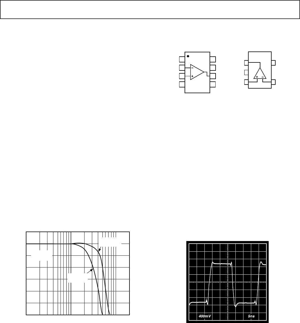
GAIN – dB
9
6
–12
10M 100M 1G
3
0
–3
–6
–9
FREQUENCY – Hz
V
S
= 5V
R
FB
= 820
V
S
= 5V
R
FB
= 1k
G = +2
R
L
= 100
Figure 1. Frequency Response of AD8001
transimpedance linearization circuitry. This allows it to drive
video loads with excellent differential gain and phase perfor-
mance on only 50 mW of power. The AD8001 is a current
feedback amplifier and features gain flatness of 0.1 dB to 100 MHz
while offering differential gain and phase error of 0.01% and
0.025°. This makes the AD8001 ideal for professional video
electronics such as cameras and video switchers. Additionally,
the AD8001’s low distortion and fast settling make it ideal for
buffer high speed A-to-D converters.
The AD8001 offers low power of 5.5 mA max (V
S
= ±5 V) and
can run on a single +12 V power supply, while being capable of
delivering over 70 mA of load current. These features make this
amplifier ideal for portable and battery-powered applications
where size and power are critical.
The outstanding bandwidth of 800 MHz along with 1200 V/µs
of slew rate make the AD8001 useful in many general-purpose
high speed applications where dual power supplies of up to ±6 V
and single supplies from 6 V to 12 V are needed. The AD8001 is
available in the industrial temperature range of –40°C to +85°C.
Figure 2. Transient Response of AD8001; 2 V Step, G = +2
8-Lead PDIP (N-8),
CERDIP (Q-8) and SOIC (R-8)
5-Lead SOT-23-5
(RT-5)
FUNCTIONAL BLOCK DIAGRAMS
AD8001* PRODUCT PAGE QUICK LINKS
Last Content Update: 02/23/2017
COMPARABLE PARTS
View a parametric search of comparable parts.
EVALUATION KITS
Universal Evaluation Board for Single High Speed
Operational Amplifiers
DOCUMENTATION
Application Notes
AN-253: Find Op Amp Noise with Spreadsheet
AN-257: Careful Design Tames High Speed Op Amps
AN-356: User's Guide to Applying and Measuring
Operational Amplifier Specifications
AN-358: Noise and Operational Amplifier Circuits
AN-417: Fast Rail-to-Rail Operational Amplifiers Ease
Design Constraints in Low Voltage High Speed Systems
AN-649: Using the Analog Devices Active Filter Design
Tool
AN-692: Universal Precision Op Amp Evaluation Board
Data Sheet
AD8001: 800 MHz, 50mW Current Feedback Amplifier
Data Sheet
AD8001: Military Data Sheet
User Guides
UG-755: 8-Lead SOIC Amplifier Evaluation Board User
Guide
UG-838: Evaluation Board for Single, High Speed Op Amps
Offered in 5-Lead SOT-23 and 6-Lead SOT-23 Packages
TOOLS AND SIMULATIONS
Analog Filter Wizard
Analog Photodiode Wizard
AD8001 SPICE Macro Model
REFERENCE MATERIALS
Product Selection Guide
High Speed Amplifiers Selection Table
Tutorials
MT-034: Current Feedback (CFB) Op Amps
MT-051: Current Feedback Op Amp Noise Considerations
MT-057: High Speed Current Feedback Op Amps
MT-059: Compensating for the Effects of Input
Capacitance on VFB and CFB Op Amps Used in Current-to-
Voltage Converters
DESIGN RESOURCES
AD8001 Material Declaration
PCN-PDN Information
Quality And Reliability
Symbols and Footprints
DISCUSSIONS
View all AD8001 EngineerZone Discussions.
SAMPLE AND BUY
Visit the product page to see pricing options.
TECHNICAL SUPPORT
Submit a technical question or find your regional support
number.
DOCUMENT FEEDBACK
Submit feedback for this data sheet.
This page is dynamically generated by Analog Devices, Inc., and inserted into this data sheet. A dynamic change to the content on this page will not
trigger a change to either the revision number or the content of the product data sheet. This dynamic page may be frequently modified.
REV. D
–2–
AD8001–SPECIFICATIONS
(@ T
A
= + 25C, V
S
= 5 V, R
L
= 100
, unless otherwise noted.)
AD8001A
Model Conditions Min Typ Max Unit
DYNAMIC PERFORMANCE
–3 dB Small Signal Bandwidth, N Package G = +2, < 0.1 dB Peaking, R
F
= 750 350 440 MHz
G=+1, < 1 dB Peaking, R
F
= 1 k 650 880 MHz
R Package G = +2, < 0.1 dB Peaking, R
F
= 681 350 440 MHz
G=+1, < 0.1 dB Peaking, R
F
= 845 575 715 MHz
RT Package G = +2, < 0.1 dB Peaking, R
F
= 768 300 380 MHz
G=+1, < 0.1 dB Peaking, R
F
= 1 k 575 795 MHz
Bandwidth for 0.1 dB Flatness
N Package G = +2, R
F
= 750 85 110 MHz
R Package G = +2, R
F
= 681 100 125 MHz
RT Package G = +2, R
F
= 768 120 145 MHz
Slew Rate G = +2, V
O
= 2 V Step 800 1000 V/µs
G = –1, V
O
= 2 V Step 960 1200 V/µs
Settling Time to 0.1% G = –1, V
O
= 2 V Step 10 ns
Rise and Fall Time G = +2, V
O
= 2 V Step, R
F
= 649 1.4 ns
NOISE/HARMONIC PERFORMANCE
Total Harmonic Distortion f
C
= 5 MHz, V
O
= 2 V p-p –65 dBc
G = +2, R
L
= 100
Input Voltage Noise f = 10 kHz 2.0 nV/Hz
Input Current Noise f = 10 kHz, +In 2.0 pA/Hz
–In 18 pA/Hz
Differential Gain Error NTSC, G = +2, R
L
= 150 0.01 0.025 %
Differential Phase Error NTSC, G = +2, R
L
= 150 0.025 0.04 Degree
Third Order Intercept f = 10 MHz 33 dBm
1 dB Gain Compression f = 10 MHz 14 dBm
SFDR f = 5 MHz –66 dB
DC PERFORMANCE
Input Offset Voltage 2.0 5.5 mV
T
MIN
–T
MAX
2.0 9.0 mV
Offset Drift 10 µV/°C
–Input Bias Current 5.0 25 ±µA
T
MIN
–T
MAX
35 ±µA
+Input Bias Current 3.0 6.0 ±µA
T
MIN
–T
MAX
10 ±µA
Open-Loop Transresistance V
O
= ±2.5 V 250 900 k
T
MIN
–T
MAX
175 k
INPUT CHARACTERISTICS
Input Resistance +Input 10 M
–Input 50
Input Capacitance +Input 1.5 pF
Input Common-Mode Voltage Range 3.2 ±V
Common-Mode Rejection Ratio
Offset Voltage V
CM
= ±2.5 V 50 54 dB
–Input Current V
CM
= ±2.5 V, T
MIN
–T
MAX
0.3 1.0 µA/V
+Input Current V
CM
= ±2.5 V, T
MIN
–T
MAX
0.2 0.7 µA/V
OUTPUT CHARACTERISTICS
Output Voltage Swing R
L
= 150 2.7 3.1 ±V
Output Current R
L
= 37.5 50 70 mA
Short Circuit Current 85 110 mA
POWER SUPPLY
Operating Range ±3.0 ±6.0 V
Quiescent Current T
MIN
–T
MAX
5.0 5.5 mA
Power Supply Rejection Ratio +V
S
= +4 V to +6 V, –V
S
= –5 V 60 75 dB
–V
S
= – 4 V to –6 V, +V
S
= +5 V 50 56 dB
–Input Current T
MIN
–T
MAX
0.5 2.5 µA/V
+Input Current T
MIN
–T
MAX
0.1 0.5 µA/V
Specifications subject to change without notice.

AD8001ARZ

Mfr. #:
Manufacturer:
Analog Devices Inc.
Description:
Video Amplifiers 800MHz 50mW Current Feedback
Lifecycle:
New from this manufacturer.
Delivery:
DHL FedEx Ups TNT EMS
Payment:
T/T Paypal Visa MoneyGram Western Union