REV. D
AD8001
–11–
Printed Circuit Board Layout Considerations
As to be expected for a wideband amplifier, PC board parasitics
can affect the overall closed-loop performance. Of concern are
stray capacitances at the output and the inverting input nodes. If
a ground plane is to be used on the same side of the board as
the signal traces, a space (5 mm min) should be left around the
signal lines to minimize coupling. Additionally, signal lines
connecting the feedback and gain resistors should be short
enough so that their associated inductance does not cause high
frequency gain errors. Line lengths on the order of less than
5 mm are recommended. If long runs of coaxial cable are being
driven, dispersion and loss must be considered.
Power Supply Bypassing
Adequate power supply bypassing can be critical when optimiz-
ing the performance of a high frequency circuit. Inductance in
the power supply leads can form resonant circuits that produce
peaking in the amplifier’s response. In addition, if large current
transients must be delivered to the load, then bypass capacitors
(typically greater than 1 µF) will be required to provide the best
settling time and lowest distortion. A parallel combination of
4.7 µF and 0.1 µF is recommended. Some brands of electrolytic
capacitors will require a small series damping resistor ≈4.7 Ω for
optimum results.
DC Errors and Noise
There are three major noise and offset terms to consider in a
current feedback amplifier. For offset errors, refer to the equation
below. For noise error the terms are root-sum-squared to give a
net output error. In the circuit in Figure 7 they are input offset
(V
IO
), which appears at the output multiplied by the noise gain
of the circuit (1 + R
F
/R
I
), noninverting input current (I
BN
× R
N
)
also multiplied by the noise gain, and the inverting input current,
which when divided between R
F
and R
I
and subsequently
multiplied by the noise gain always appears at the output as
I
BN
× R
F
. The input voltage noise of the AD8001 is a low 2 nV/
√Hz. At low gains though the inverting input current noise times
R
F
is the dominant noise source. Careful layout and device
matching contribute to better offset and drift specifications for
the AD8001 compared to many other current feedback ampli-
fiers. The typical performance curves in conjunction with the
following equations can be used to predict the performance of
the AD8001 in any application.
VV
R
R
IR
R
R
IR
OUT IO
F
I
BN N
F
I
BI F
=×+
±××+
±×11
R
F
R
I
R
N
I
BN
V
OUT
I
BI
Figure 7. Output Offset Voltage
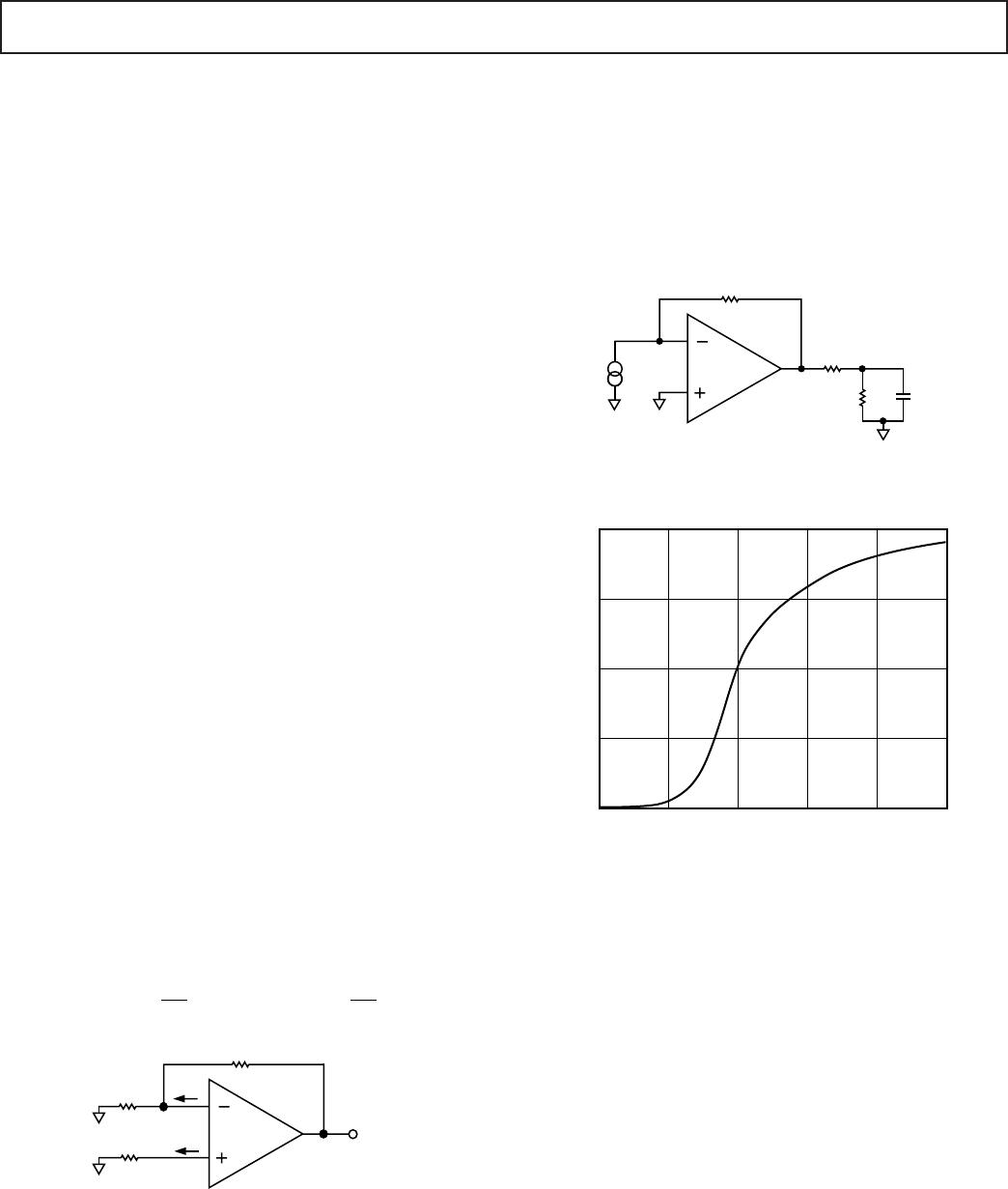
Driving Capacitive Loads
The AD8001 was designed primarily to drive nonreactive loads.
If driving loads with a capacitive component is desired, best
frequency response is obtained by the addition of a small series
resistance, as shown in Figure 8. The accompanying graph
shows the optimum value for R
SERIES
versus capacitive load. It is
worth noting that the frequency response of the circuit when
driving large capacitive loads will be dominated by the passive
roll-off of R
SERIES
and C
L
.
909
R
SERIES
R
L
500
I
N
C
L
Figure 8. Driving Capacitive Loads
40
0
0
25
30
10
5
20
15 2010
C
L
– pF
G = +1
R
SERIES
–
Figure 9. Recommended R
SERIES
vs. Capacitive Load