REV. D
AD8001
–14–
Layout Considerations
The specified high speed performance of the AD8001 requires
careful attention to board layout and component selection. Proper
R
F
design techniques and low parasitic component selection
are mandatory.
The PCB should have a ground plane covering all unused portions
of the component side of the board to provide a low impedance
ground path. The ground plane should be removed from the area
near the input pins to reduce stray capacitance.
Chip capacitors should be used for supply bypassing (see Figure 13).
One end should be connected to the ground plane and the other
within 1/8 inch of each power pin. An additional large
(4.7 µF–10 µF) tantalum electrolytic capacitor should be con-
nected in parallel, but not necessarily so close, to supply current
for fast, large-signal changes at the output.
The feedback resistor should be located close to the inverting
input pin in order to keep the stray capacitance at this node to a
minimum. Capacitance variations of less than 1 pF at the invert-
ing input will significantly affect high speed performance.
Stripline design techniques should be used for long signal traces
(greater than about 1 inch). These should be designed with a
characteristic impedance of 50 Ω or 75 Ω and be properly termi-
nated at each end.
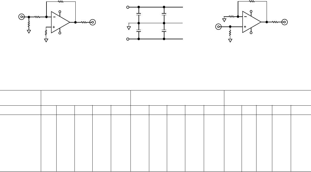
Inverting Configuration Supply Bypassing
C1
0.1F
C2
0.1F
+V
S
–V
S
C3
10F
C4
10F
Noninverting Configuration
R
F
R
O
IN
+V
S
–V
S
R
S
R
T
R
G
OUT
R
F
R
O
IN
+V
S
–V
S
R
T
R
G
OUT
Figure 13. Inverting and Noninverting Configurations for Evaluation Boards
Table I. Recommended Component Values
AD8001AN (PDIP) AD8001AR (SOIC) AD8001ART (SOT-23-5)
Gain Gain Gain
Component –1 +1 +2 +10 +100 –1 +1 +2 +10 +100 –1 +1 +2 +10 +100
R
F
(Ω) 649 1050 750 470 1000 604 953 681 470 1000 845 1000 768 470 1000
R
G
(Ω) 649 750 51 10 604 681 51 10 845 768 51 10
R
O
(Nominal) (Ω) 49.9 49.9 49.9 49.9 49.9 49.9 49.9 49.9 49.9 49.9 49.9 49.9 49.9 49.9 49.9
R
S
(Ω)0 0 0
R
T
(Nominal) (Ω) 54.9 49.9 49.9 49.9 49.9 54.9 49.9 49.9 49.9 49.9 54.9 49.9 49.9 49.9 49.9
Small Signal 340 880 460 260 20 370 710 440 260 20 240 795 380 260 20
BW (MHz)
0.1 dB Flatness 105 70 105 130 100 120 110 300 145
(MHz)