LTC2636
13
2636fc
For more information www.linear.com/LTC2636
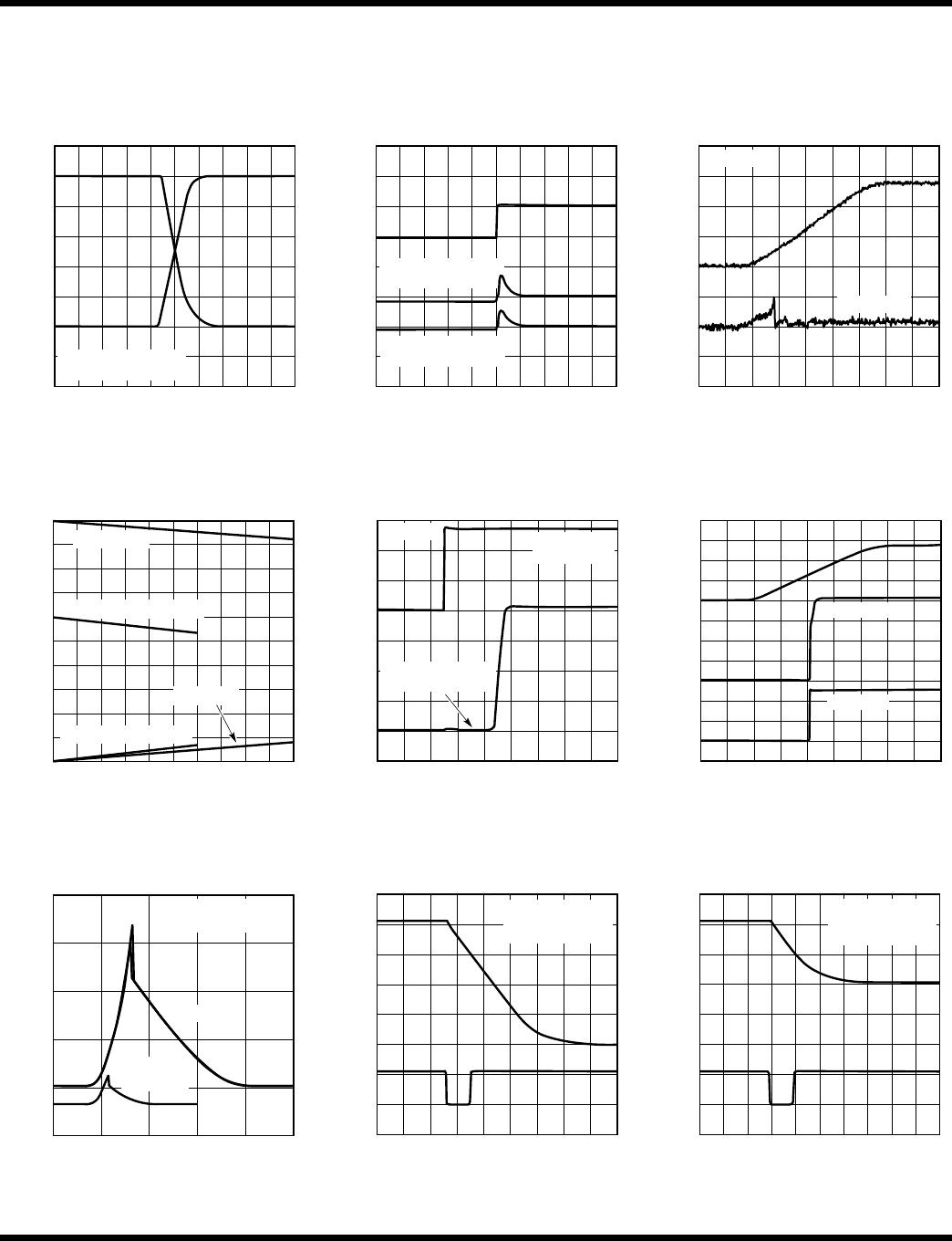
TYPICAL PERFORMANCE CHARACTERISTICS
Large-Signal Response
Headroom at Rails
vs Output Current
Mid-Scale Glitch Impulse Power-On Reset Glitch
Power-On Reset to Mid-ScaleExiting Power-Down to Mid-Scale
Supply Current vs Logic Voltage Hardware CLR Hardware CLR to Mid-Scale
T
A
= 25°C, unless otherwise noted.
LTC2636
2µs/DIV
V
OUT
0.5V/DIV
2636 G22
V
FS
= V
CC
= 5V
1/4 SCALE to 3/4 SCALE
2µs/DIV
V
OUT
5mV/DIV
CS/LD
5V/DIV
2636 G23
LTC2636-H12, V
CC
= 5V
3.0nV•s TYP
LTC2636-L12, V
CC
= 3V
2.1nV•s TYP
200µs/DIV
V
OUT
5mV/DIV
V
CC
2V/DIV
2636 G24
LTC2636-L
ZERO-SCALE
I
OUT
(mA)
0
V
OUT
(V)
5.0
4.5
1.0
1.5
2.0
2.5
3.0
3.5
4.0
0.5
0
1
2636 G25
2 3 4 5 6 7 8 9 10
5V SOURCING
3V (LTC2636-L) SOURCING
5V SINKING
3V (LTC2636-L) SINKING
5µs/DIV
V
OUT
0.5V/DIV
CS/LD
2V/DIV
2636 G26
LTC2636-H
V
CC
= 5V
INTERNAL REF.
DACs A-G IN
POWER-DOWN MODE
200µs/DIV
V
CC
2V/DIV
V
OUT
0.5V/DIV
2636 G27
LTC2636-H
LTC2636-L
LOGIC VOLTAGE (V)
0
I
CC
(mA)
1.5
1.2
1.4
1.0
0.8
0.6
2636 G28
54321
SWEEP SCK, SDI, CS/LD
BETWEEN 0V AND V
CC
V
CC
= 5V
V
CC
= 3V
(LTC2636-L)
1µs/DIV
CLR
5V/DIV
V
OUT
1V/DIV
2636 G29
V
CC
= 5V
V
REF
= 4.096V
CODE = FULL-SCALE
1µs/DIV
V
OUT
1V/DIV
CLR
5V/DIV
2636 G30
V
CC
= 5V
V
REF
= 4.096V
CODE = FULL-SCALE
LTC2636
14
2636fc
For more information www.linear.com/LTC2636
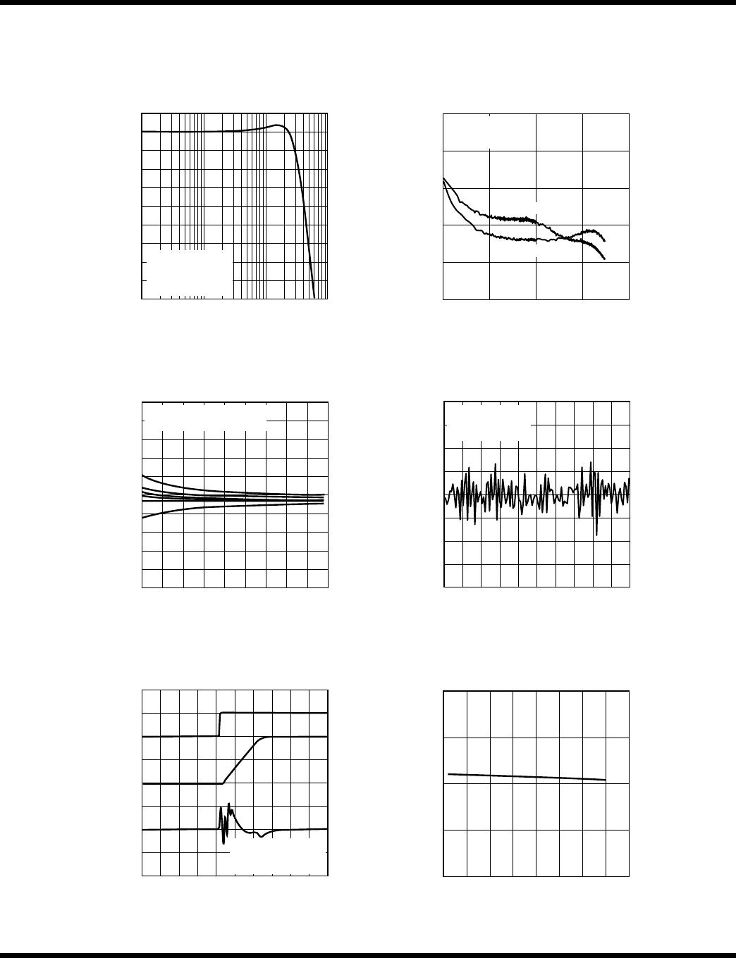
TYPICAL PERFORMANCE CHARACTERISTICS
Multiplying Bandwidth
Gain Error vs Reference Input
Noise Voltage vs Frequency
0.1Hz to 10Hz Voltage Noise
DAC to DAC Crosstalk (Dynamic) Gain Error vs Temperature
T
A
= 25°C, unless otherwise noted.
LTC2636
FREQUENCY (Hz)
dB
2636 G31
2
0
–16
–14
–12
–10
–8
–6
–4
–2
–18
1k 100k 1M10k
V
CC
= 5V
V
REF(DC)
= 2V
V
REF(AC)
= 0.2V
P-P
CODE = FULL-SCALE
FREQUENCY (Hz)
100
NOISE VOLTAGE (nV/√Hz)
500
400
300
200
100
0
1k 100k
2636 G32
1M10k
V
CC
= 5V
CODE = MID-SCALE
INTERNAL REF.
LTC2636-H
LTC2636-L
REFERENCE VOLTAGE (V)
1
GAIN ERROR (%FSR)
1.0
0.8
0.6
0.4
–0.6
–0.8
–0.4
–0.2
0.2
0
–1.0
1.5 4 5.4 5
2636 G33
5.52 2.533.5
V
CC
= 5.5V
GAIN ERROR OF 8 CHANNELS
1s/DIV
10µV/DIV
2636 G34
V
CC
= 5V, V
FS
= 2.5V
CODE = MIDSCALE
INTERNAL REF.
2µs/DIV
V
OUT
1mV/DIV
1 DAC
SWITCH 0-FS
2V/DIV
CS/LD
5V/DIV
2636 G35
LTC2636-H12, V
CC
= 5V
2.4nV•s TYP
C
REF
= 0.1µF
TEMPERATURE (°C)
–50
GAIN ERROR (%FSR)
1.0
0.5
0
–0.5
–1.0
–25 52 05 57 001 521
2636 G36
1500
LTC2636
15
2636fc
For more information www.linear.com/LTC2636
PIN FUNCTIONS
V
CC
(Pin 1/1): Supply Voltage Input. 2.7V V
CC
5.5V
(LTC2636-L) or 4.5V ≤ V
CC
5.5V (LTC2636-H). Bypass
to GND with a 0.1μF capacitor.
V
OUT
A to V
OUT
H (Pins 2-5, 10-13/2-5, 12-15): DAC
Analog Voltage Outputs.
CS/LD (Pin 6/7): Serial Interface Chip Select/Load Input.
When CS/LD is low, SCK is enabled for shifting data on
SDI into the register. When CS/LD is taken high, SCK
is disabled and the specified command (see Table 1) is
executed.
SCK (Pin 7/8): Serial Interface Clock Input. CMOS and
TTL compatible.
SDI (Pin 8/9): Serial Interface Data Input. Data on SDI
is clocked into the DAC on the rising edge of SCK. The
LTC2636 accepts input word lengths of either 24 or 32 bits.
REF (Pin 9/11): Reference Voltage Input or Output. When
External Reference mode is selected, REF is an input
(1V V
REF
V
CC
) where the voltage supplied sets the
full-scale DAC output voltage. When Internal Reference
is selected, the 10ppm/°C 1.25V (LTC2636-L) or 2.048V
(LTC2636-H) internal reference (half full-scale) is avail
-
able at REF. This output may be bypassed to GND with up
to 10μF, and must be buffered when driving external DC
load current.
GND (Pin 14/16): Ground.
LDAC (Pin 6, MSOP only): Asynchronous DAC Update
Pin. If CS/LD is high, a falling edge on LDAC immediately
updates the DAC registers with the contents of the input
registers (similar to a software update). If CS/LD is low
when LDAC goes low, the DAC registers are updated after
CS/LD returns high. A low on the LDAC pin powers up
the DACs. A software power down command is ignored if
LDAC is low. If the LDAC functionality is not being used,
the LDAC pin should be tied high.
CLR (Pin 10, MSOP only): Asynchronous Clear Input.
A logic low at this level-triggered input clears all regis-
ters and causes the DAC voltage output to reset to Zero
(LTC2636-Z) or Mid-scale (LTC2636-MI/-MX). CMOS and
TTL compatible.
Exposed Pad (Pin 15, DFN Only): Ground. Must be sol-
dered to PCB Ground.
(DFN/MSOP)
LTC2636IMS-HZ10#TRPBF

Mfr. #:
Manufacturer:
Analog Devices Inc.
Description:
Digital to Analog Converters - DAC 10-Bit SPI Octal DAC (4.096V ref, Reset to Zero-Scale)
Lifecycle:
New from this manufacturer.
Delivery:
DHL FedEx Ups TNT EMS
Payment:
T/T Paypal Visa MoneyGram Western Union