LTC2636
7
2636fc
For more information www.linear.com/LTC2636
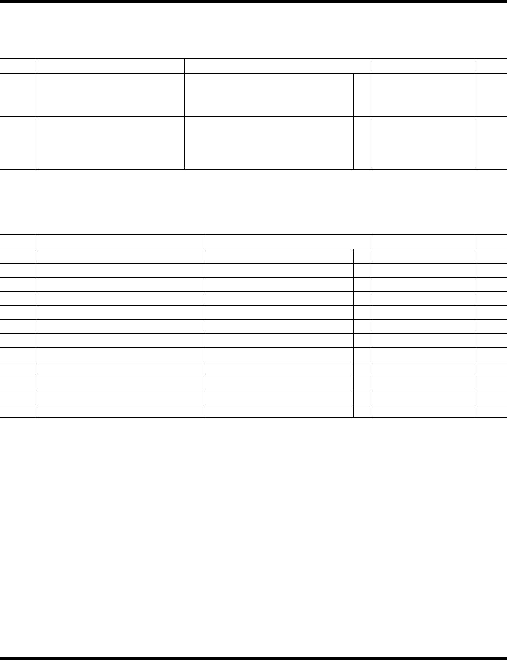
LTC2636-LMI12/-LMI10/-LMI8/-LMX12/-LMX10/-LMX8/-LZ12/-LZ10/-LZ8 (V
FS
= 2.5V)
SYMBOL PARAMETER CONDITIONS MIN TYP MAX UNITS
t1 SDI Valid to SCK Setup
l
4 ns
t2 SDI Valid to SCK Hold
l
4 ns
t3 SCK High Time
l
9 ns
t4 SCK Low Time
l
9 ns
t5 CS/LD Pulse Width
l
10 ns
t6 LSB SCK High to CS/LD High
l
7 ns
t7 CS/LD Low to SCK High
l
7 ns
t8 CLR Pulse Width
l
20 ns
t9 LDAC Pulse Width
l
15 ns
t10 CS/LD High to SCK Positive Edge
l
7 ns
SCK Frequency 50% Duty Cycle
l
50 MHz
t11 CS/LD High to LDAC High or Low Transition
l
200 ns
TIMING CHARACTERISTICS
The l denotes the specifications which apply over the full operating temperature
range, otherwise specifications are at T
A
= 25°C. V
CC
= 2.7V to 5.5V, V
OUT
unloaded unless otherwise specified.
ELECTRICAL CHARACTERISTICS
The l denotes the specifications which apply over the full operating
temperature range, otherwise specifications are at T
A
= 25°C. V
CC
= 4.5V to 5.5V, V
OUT
unloaded unless otherwise specified.
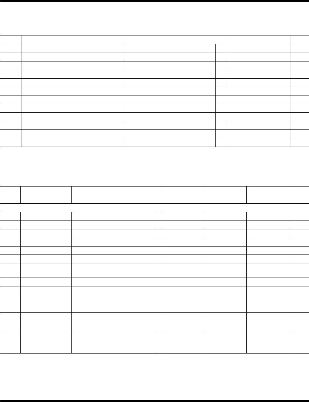
LTC2636-HMI12/-HMI10/-HMI8/-HMX12/-HMX10/-HMX8/-HZ12/-HZ10/-HZ8 (V
FS
= 4.096V)
SYMBOL PARAMETER CONDITIONS
LTC2636-8 LTC2636-10 LTC2636-12
UNITSMIN TYP MAX MIN TYP MAX MIN TYP MAX
DC Performance
Resolution
l
8 10 12 Bits
Monotonicity V
CC
= 5V, Internal Reference (Note 4)
l
8 10 12 Bits
DNL Differential Nonlinearity V
CC
= 5V, Internal Reference (Note 4)
l
±0.5 ±0.5 ±1 LSB
INL Integral Nonlinearity V
CC
= 5V, Internal Reference (Note 4)
l
±0.05 ±0.5 ±0.2 ±1 ±1 ±2.5 LSB
ZSE Zero-Scale Error V
CC
= 5V, Internal Reference, Code = 0
l
0.5 5 0.5 5 0.5 5 mV
V
OS
Offset Error V
CC
= 5V, Internal Reference (Note 5)
l
±0.05 ±5 ±0.05 ±5 ±0.05 ±5 mV
V
OSTC
V
OS
Temperature
Coefficient
V
CC
= 5V, Internal Reference ±10 ±10 ±10 µV/°C
GE Gain Error V
CC
= 5V, Internal Reference
l
±0.2 ±0.8 ±0.2 ±0.8 ±0.2 ±0.8 %FSR
GE
TC
Gain Temperature
Coefficient
V
CC
= 5V, Internal Reference (Note 10)
C-Grade
I-Grade
H-Grade
10
10
10
10
10
10
10
10
10
ppm/°C
ppm/°C
ppm/°C
Load Regulation V
CC
= 5V±10%, (Note 11)
Internal Reference, Mid-Scale,
–10mA ≤ I
OUT
≤ 10mA
l
0.006 0.01 0.022 0.04 0.09 0.16 LSB/mA
R
OUT
DC Output Impedance V
CC
= 5V±10%, (Note 11)
Internal Reference, Mid-Scale,
–10mA ≤ I
OUT
≤ 10mA
l
0.09 0.156 0.09 0.156 0.09 0.156 Ω
LTC2636
8
2636fc
For more information www.linear.com/LTC2636
SYMBOL PARAMETER CONDITIONS MIN TYP MAX UNITS
V
OUT
DAC Output Span External Reference
Internal Reference
0 to V
REF
0 to 4.096
V
V
PSR Power Supply Rejection V
CC
= 5V±10% –80 dB
I
SC
Short Circuit Output Current (Note 6)
Sinking
Sourcing
V
FS
= V
CC
= 5.5V
Zero-Scale; V
OUT
Shorted to V
CC
Full-Scale; V
OUT
Shorted to GND
l
l
27
–28
48
–48
mA
mA
Power Supply
V
CC
Positive Supply Voltage For Specified Performance
l
4.5 5.5 V
I
CC
Supply Current (Note 7) V
CC
= 5V, V
REF
= 4.096V, External Reference
V
CC
= 5V, Internal Reference
l
l
1.0
1.1
1.3
1.5
mA
mA
I
SD
Supply Current in Power-Down Mode
(Note 7)
V
CC
= 5V, C-Grade, I-Grade
V
CC
= 5V, H-Grade
l
l
0.5
0.5
20
30
µA
µA
Reference Input
V
REF
Input Voltage Range
l
1 V
CC
V
Resistance
l
120 160 200
Capacitance 12 pF
I
REF
Reference Current, Power-Down Mode DAC Powered Down
l
0.005 1.5 µA
Reference Output
Output Voltage
l
2.032 2.048 2.064 V
Reference Temperature Coefficient ±10 ppm/°C
Output Impedance 0.5
Capacitive Load Driving 10 µF
Short Circuit Current V
CC
= 5.5V; REF Shorted to GND 4 mA
Digital I/O
V
IH
Digital Input High Voltage
l
2.4 V
V
IL
Digital Input Low Voltage
l
0.8 V
I
LK
Digital Input Leakage V
IN
= GND to V
CC
l
±1 µA
C
IN
Digital Input Capacitance (Note 8)
l
2.5 pF
AC Performance
t
S
Settling Time V
CC
= 5V (Note 9)
±0.39% (±1LSB at 8 Bits)
±0.098% (±1LSB at 10 Bits)
±0.024% (±1LSB at 12 Bits)
3.8
4.3
4.8
µs
µs
µs
Voltage Output Slew Rate 1.0 V/µs
Capacitive Load Driving 500 pF
Glitch Impulse At Mid-Scale T
ransition 3.0 nV•s
DAC-to-DAC Crosstalk 1 DAC held at FS, 1 DAC Switch 0-FS 2.4 nV•s
Multiplying Bandwidth External Reference 320 kHz
ELECTRICAL CHARACTERISTICS
The l denotes the specifications which apply over the full operating
temperature range, otherwise specifications are at T
A
= 25°C. V
CC
= 4.5V to 5.5V, V
OUT
unloaded unless otherwise specified.
LTC2636-HMI12/-HMI10/-HMI8/-HMX12/-HMX10/-HMX8/-HZ12/-HZ10/-HZ8 (V
FS
= 4.096V)
LTC2636
9
2636fc
For more information www.linear.com/LTC2636
SYMBOL PARAMETER CONDITIONS MIN TYP MAX UNITS
e
n
Output Voltage Noise Density At f = 1kHz, External Reference
At f = 10kHz, External Reference
At f = 1kHz, Internal Reference
At f = 10kHz, Internal Reference
180
160
250
230
nV/√
Hz
nV/√Hz
nV/√Hz
nV/√Hz
Output Voltage Noise 0.1Hz to 10Hz, External Reference
0.1Hz to 10Hz, Internal Reference
0.1Hz to 200kHz, External Reference
0.1Hz to 200kHz, Internal Reference
C
REF
= 0.1μF
35
50
680
750
µV
P-P
µV
P-P
µV
P-P
µV
P-P
ELECTRICAL CHARACTERISTICS
The l denotes the specifications which apply over the full operating
temperature range, otherwise specifications are at T
A
= 25°C. V
CC
= 4.5V to 5.5V, V
OUT
unloaded unless otherwise specified.
LTC2636-HMI12/-HMI10/-HMI8/-HMX12/-HMX10/-HMX8/-HZ12/-HZ10/-HZ8 (V
FS
= 4.096V)
LTC2636-HMI12/-HMI10/-HMI8/-HMX12/-HMX10/-HMX8/-HZ12/-HZ10/-HZ8 (V
FS
= 4.096V)
SYMBOL PARAMETER CONDITIONS MIN TYP MAX UNITS
t1 SDI Valid to SCK Setup
l
4 ns
t2 SDI Valid to SCK Hold
l
4 ns
t3 SCK High Time
l
9 ns
t4 SCK Low Time
l
9 ns
t5 CS/LD Pulse Width
l
10 ns
t6 LSB SCK High to CS/LD High
l
7 ns
t7 CS/LD Low to SCK High
l
7 ns
t8 CLR Pulse Width
l
20 ns
t9 LDAC Pulse Width
l
15 ns
t10 CS/LD High to SCK Positive Edge
l
7 ns
SCK Frequency 50% Duty Cycle
l
50 MHz
t11 CS/LD High to LDAC High or Low Transition
l
200 ns
TIMING CHARACTERISTICS
The l denotes the specifications which apply over the full operating temperature
range, otherwise specifications are at T
A
= 25°C. V
CC
= 4.5V to 5.5V, V
OUT
unloaded unless otherwise specified.
Note 1: Stresses beyond those listed under Absolute Maximum Ratings
may cause permanent damage to the device. Exposure to any Absolute
Maximum Rating condition for extended periods may affect device
reliability and lifetime.
Note 2: All voltages are with respect to GND.
Note 3: High temperatures degrade operating lifetimes. Operating lifetime
is derated at temperatures greater than 105°C. Operating at temperatures
above 110°C and with V
CC
> 4V requires V
CC
slew rates to be no greater
than 110mV/µs.
Note 4: Linearity and monotonicity are defined from code kL to code 2
N
–1,
where N is the resolution and k
L
is given by kL = 0.016•(2
N
/V
FS
), rounded
to the nearest whole code. For V
FS
= 2.5V and N = 12, k
L
= 26 and linearity
is defined from code 26 to code 4,095. For V
FS
= 4.096V and N = 12, k
L
=
16 and linearity is defined from code 16 to code 4,095.
Note 5: Inferred from measurement at code 16 (LTC2636-12), code 4
(LTC2636-10) or code 1 (LTC2636-8), and at full-scale.
Note 6: This IC includes current limiting that is intended to protect the
device during momentary overload conditions. Junction temperature can
exceed the rated maximum during current limiting. Continuous operation
above the specified maximum operating junction temperature may impair
device reliability.
Note 7: Digital inputs at 0V or V
CC
.
Note 8: Guaranteed by design and not production tested.
Note 9: Internal Reference mode. DAC is stepped 1/4 scale to 3/4 scale
and 3/4 scale to 1/4 scale. Load is 2kΩ in parallel with 100pF to GND.
Note 10: Temperature coefficient is calculated by dividing the maximum
change in output voltage by the specified temperature range.
Note 11: Thermal resistance of MSOP package limits I
OUT
to
–5mA ≤ I
OUT
≤ 5mA for H-grade MSOP parts and V
CC
= 5V ±10%.
LTC2636IMS-HZ10#TRPBF

Mfr. #:
Manufacturer:
Analog Devices Inc.
Description:
Digital to Analog Converters - DAC 10-Bit SPI Octal DAC (4.096V ref, Reset to Zero-Scale)
Lifecycle:
New from this manufacturer.
Delivery:
DHL FedEx Ups TNT EMS
Payment:
T/T Paypal Visa MoneyGram Western Union