AS7C316098A-10BINTR

AS7C316098A
Rev. 1.2
1024K X 16 BIT HIGH SPEED CMOS SRAM
REVISION HISTORY
Revision Description Issue Date
Rev. 1.0
Rev. 1.1
Initial Issued
Add 48 pin BGA package type.
Jan.09. 2012
Mar.12. 2012
Rev. 1.2
1.“CE# V
CC
- 0.2V” revised as ”CE# 0.2” for TEST
CONDITION of Average Operating Power supply Current
Icc1 on page3
2.Revised ORDERING INFORMATION Page11
July.19. 2012
Alliance Memory, Inc.
0
SYMBOL
DESCRIPTION
A0 - A19
Address Inputs
DQ0 DQ15
Data Inputs/Outputs
CE#
Chip Enable Input
WE#
Write Enable Input
OE#
Output Enable Input
LB#
Lower Byte Control
UB#
Upper Byte Control
V
CC
Power Supply
V
SS
Ground
AS7C316098A
Rev. 1.2
1024K X 16 BIT HIGH SPEED CMOS SRAM
FEATURES
Fast access time : 10ns
low power consumption:
Operating current:
90mA (typical)
Standby current:
4mA(Typical)
Single 3.3V power supply
All inputs and outputs TTL compatible
Fully static operation
Tri-state output
Data byte control : LB# (DQ0 ~ DQ7)
UB# (DQ8 ~ DQ15)
Data retention voltage : 1.5V (MIN.)
Green package available
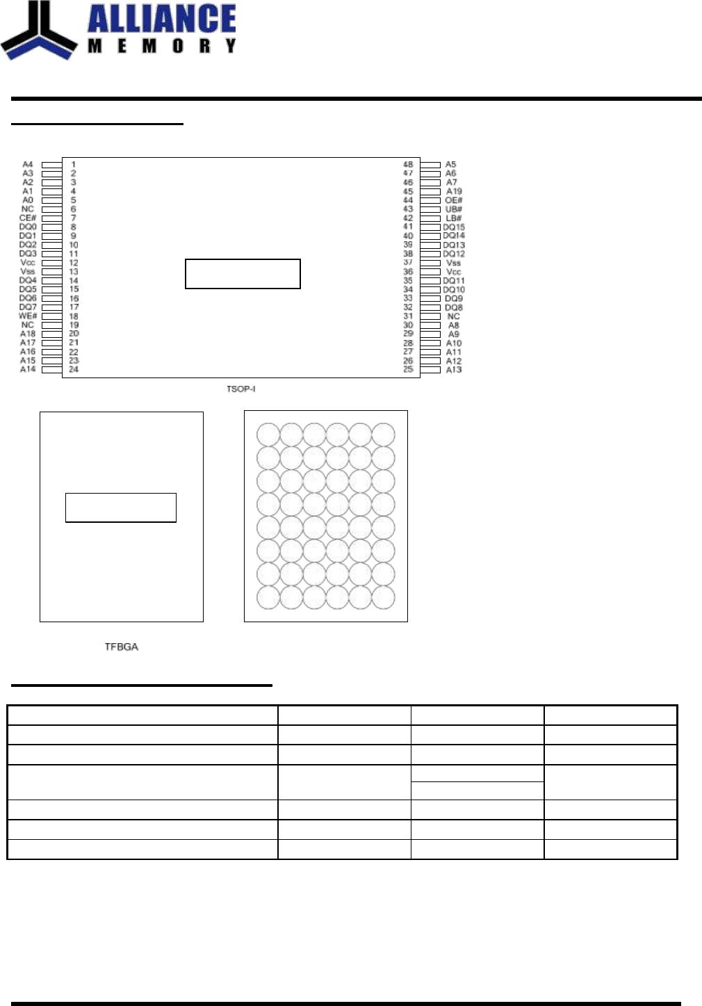
Package : 48-pin 12mm x 20mm TSOP-I
48-ball 6mmx8mm TFBGA
GENERAL DESCRIPTION
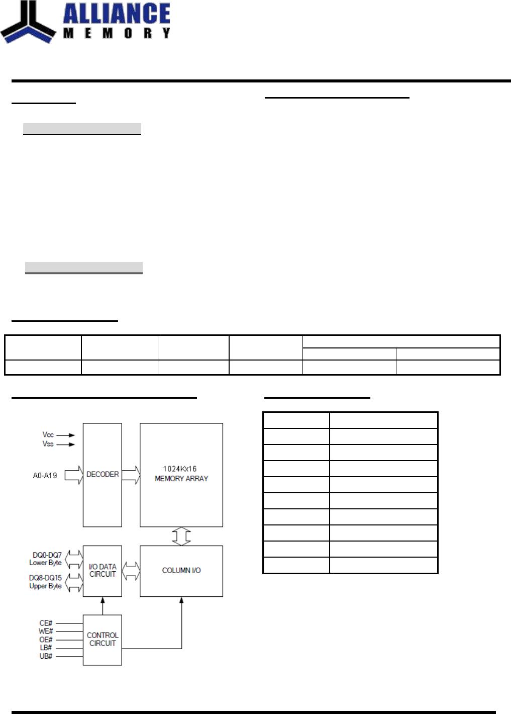
The AS7C316098A is a 16M-bit high speed CMOS
static random access memory organized as 1024K
words by 16 bits. It is fabricated using very high
performance, high reliability CMOS technology. Its
standby current is stable within the range of
operating temperature.
The AS7C316098A operates from a single
power supply of 3.3V and all inputs and outputs are
fully TTL compatible
PRODUCT FAMILY
Product
Family
Operating
Temperature
Vcc Range
Power Dissipation
Standby(ISB1,TYP.)
Operating(Icc1,TYP.)
AS7C316098A(I)
-40 ~ 85
2.7 ~ 3.6V
4mA
90mA
FUNCTIONAL BLOCK DIAGRAM PIN DESCRIPTION
Alliance Memory, Inc.
1
AS7C316098A
Rev. 1.2
1024K X 16 BIT HIGH SPEED CMOS SRAM
PIN CONFIGURATION
A
LB#
OE# A0 A1 A2 NC
B DQ8 UB#
A3
A4 CE# DQ0
C DQ9 DQ10
A5
A6 DQ1 DQ2
D Vss DQ11 A17
A7
DQ3
Vcc
E Vcc DQ12
NC
A16
DQ4
Vss
F DQ14 DQ13
A14
A15
DQ5 DQ6
G DQ15
A19
A12
A13
WE# DQ7
H A18
A8
A9
A10
A11 NC
1 2 3 4 5 6
TFBGA
ABSOLUTE MAXIMUN RATINGS*
PARAMETER
SYMBOL
RATING
UNIT
Voltage on Vcc relative to VSS
VT1
-0.5 to 4.6
V
Voltage on any other pin relative to VSS
VT2
-0.5 to Vcc+0.5
V
Operating Temperature
TA
0 to 70(C grade)
-40 to 85(I grade)
Storage Temperature
TSTG
-65 to 150
Power Dissipation
PD
1
W
DC Output Current
IOUT
50
mA
*Stresses greater than those listed under “Absolute Maximum Ratings may cause permanent damage to
the
device.
This is a stress rating
only and functional operation of the device or any other conditions above those indicated in the operational sections of this specification is not
implied. Exposure to the absolute maximum rating conditions for extended period may affect device reliability.
Alliance Memory, Inc.
2
AS7C316098A
AS7C316098A

AS7C316098A-10BINTR

Mfr. #:
Manufacturer:
Alliance Memory
Description:
SRAM 16M, 3.3V, 10ns FAST 1024K x 16 Asyn SRAM
Lifecycle:
New from this manufacturer.
Delivery:
DHL FedEx Ups TNT EMS
Payment:
T/T Paypal Visa MoneyGram Western Union