AS7C316098A
Rev. 1.2
1024K X 16 BIT HIGH SPEED CMOS SRAM
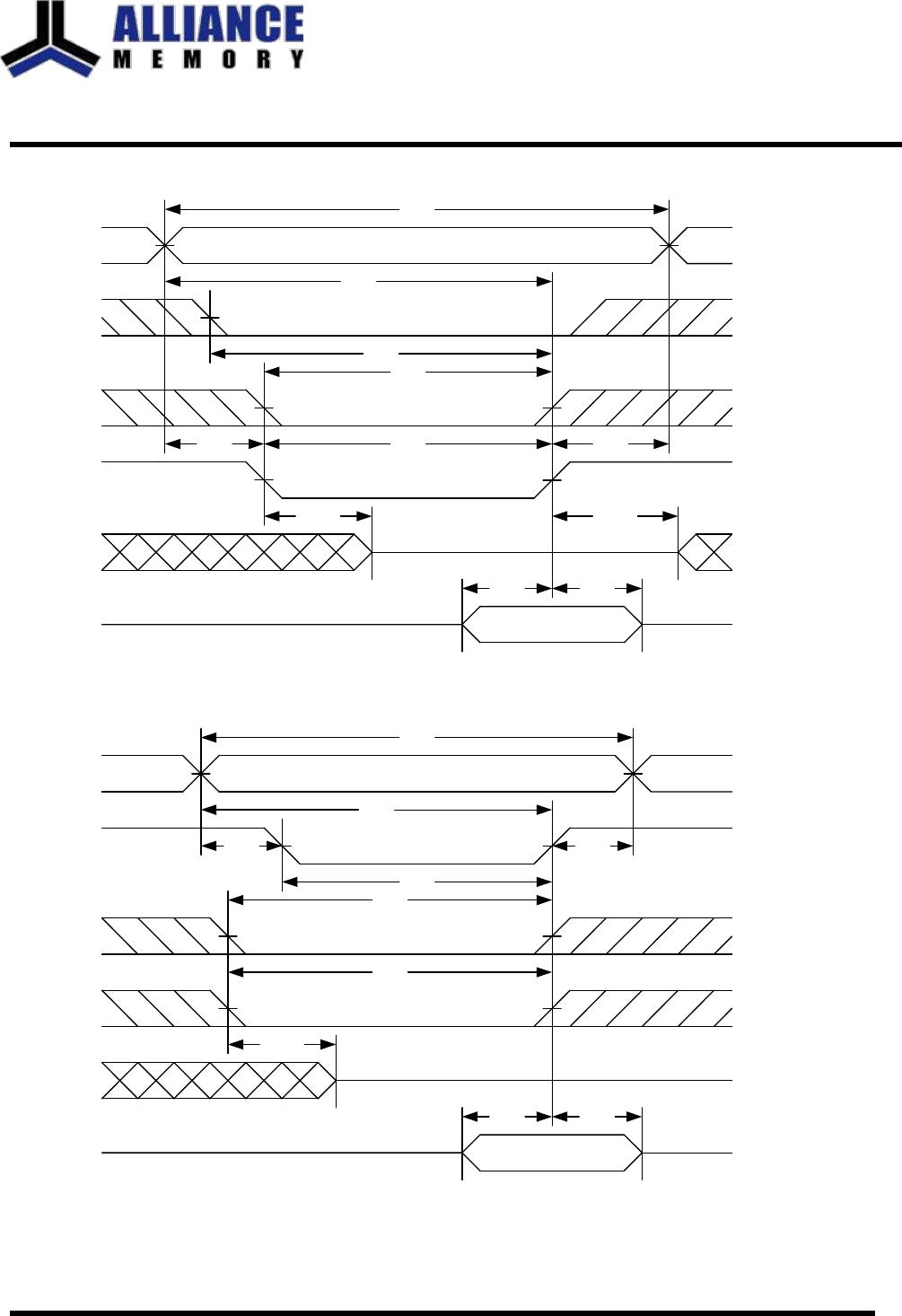
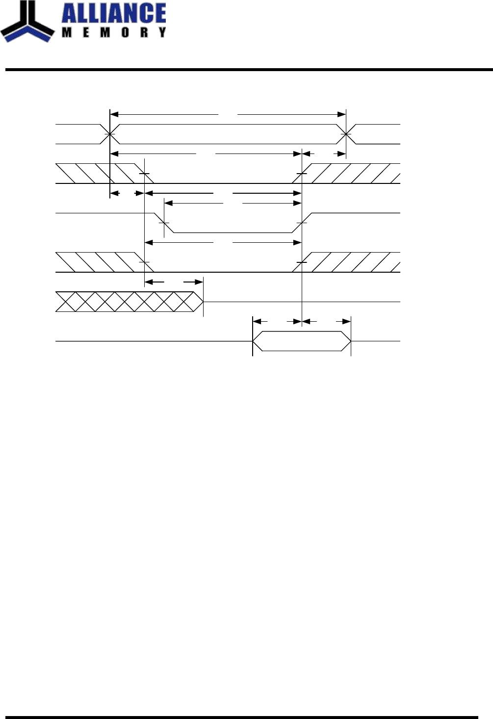
WRITE CYCLE 3 (LB#,UB# Controlled) (1,2,5,6)
t
WC
Address
t
AW
t
WR
CE#
LB#,UB#
t
AS
t
CW
t
BW
t
WP
WE#
Dout
t
WHZ
(4)
High-Z
tDW
t
DH
Din Data
Valid
Notes :
1.WE#,CE#, LB#, UB# must be high during all address transitions.
2.A write occurs during the overlap of a low CE#, low WE#, LB# or UB# = low.
3.During a WE# controlled write cycle with OE# low, tWP must be greater than tWHZ + tDW to allow the drivers to turn off and data to be placed
on the bus.
4.During this period, I/O pins are in the output state, and input signals must not be applied.
5.If the CE#, LB#, UB# low transition occurs simultaneously with or after WE# low transition, the outputs remain in a high impedance state.
6.t
OW
and t
WHZ
are specified with C
L
= 5pF. Transition is measured ±500mV from steady state.
Alliance Memory, Inc.
7