AS7C316098A-10BINTR

MODE
CE#
OE#
WE#
LB#
UB#
I/O OPERATION
SUPPLY CURRENT
DQ0-DQ7
DQ8-DQ15
Standby
H
X
X
X
X
High Z
High Z
Isb , I
SB1,
Output Disable
L
L
H
X
H
X
X
H
X
H
High Z
High Z
High Z
High Z
I
CC
Read
L
L
L
L
L
L
H
H
H
L
H
L
H
L
L
D
OUT
High Z
D
OUT
High Z
D
OUT
D
OUT
I
CC
Write
L
L
L
X
X
X
L
L
L
L
H
L
H
L
L
D
IN
High Z
D
IN
High Z
D
IN
D
IN
I
CC
PARAMETER
SYMBOL
TEST CONDITION
MIN.
TYP.
*4
MAX.
UNIT
Supply Voltage
VCC
2.7
3.3
3.6
V
Input High Voltage
*1
V
IH
2.2
-
V
CC
+0.3
V
Input Low Voltage
*2
V
IL
- 0.3
-
0.8
V
Input Leakage Current
ILI
VCC VIN VSS
- 1
-
1
µ
A
Output Leakage
Current
I
LO
V
CC
V
OUT
V
SS
,
Output Disabled
- 1
-
1
µ
A
Output High Voltage
V
OH
I
OH
= -8mA
2.4
-
-
V
Output Low Voltage
V
OL
I
OL
=4mA
-
-
0.4
V
AverageOperating
Power supply
Current
Icc
CE# = V
IL
, I
I/O
= 0mA
;f=max
-10
-
110
160
mA
Icc1
CE#
0.2, Other
pin is at 0.2V or Vcc-0.2V
I
I/O
= 0mA;f=max
-10
-
90
120
mA
Standby Power
Supply Current
Isb
CE# Vih
Other pin is at Vil or Vih
-
-
80
mA
Standby Power
Supply Current
I
SB1
CE# VCC - 0.2V;
Other pin is at 0.2V or Vcc-0.2V
-
4
40
mA
AS7C316098A
Rev. 1.2
1024K X 16 BIT HIGH SPEED CMOS SRAM
TRUTH TABLE
Note: H = VIH, L = VIL, X = Don't care.
DC ELECTRICAL CHARACTERISTICS
Notes:
1. VIH(max) = VCC + 3.0V for pulse width less than 10ns.
2. VIL(min) = VSS - 3.0V for pulse width less than 10ns.
3. Over/Undershoot specifications are characterized, not 100% tested.
4. Typical values are included for reference only and are not guaranteed or tested.
Typical valued are measured at VCC = VCC(TYP.) and TA = 25
Alliance Memory, Inc.
3
PARAMETER
SYMBOL
MIN.
MAX
UNIT
Input Capacitance
C
IN
-
8
pF
Input/Output Capacitance
CI/O
-
10
pF
PARAMETER
SYM.
AS7C316098A-10
UNIT
MIN.
MAX.
Write Cycle Time
t
WC
10
-
ns
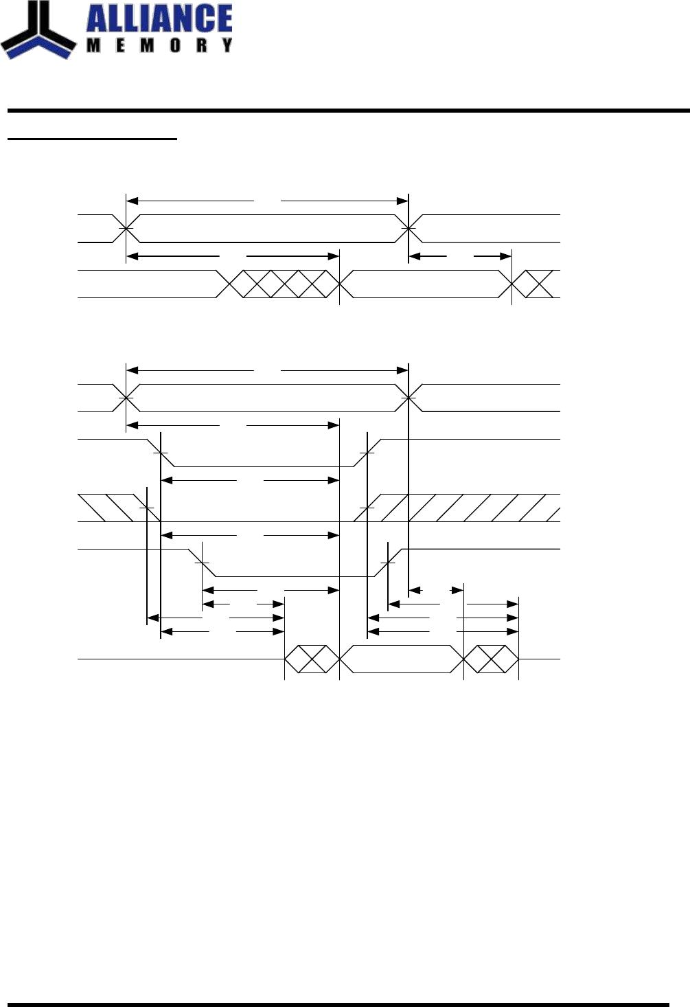
Address Valid to End of Write
t
AW
8
-
ns
Chip Enable to End of Write
t
CW
8
-
ns
Address Set-up Time
t
AS
0
-
ns
Write Pulse Width
t
WP
8
-
ns
Write Recovery Time
t
WR
0
-
ns
Data to Write Time Overlap
t
DW
6
-
ns
Data Hold from End of Write Time
t
DH
0
-
ns
Output Active from End of Write
t
OW
*
2
-
ns
Write to Output in High-Z
t
WHZ
*
-
4
ns
LB#, UB# Valid to End of Write
t
BW
8
-
ns
AS7C316098A
Rev. 1.2
1024K X 16 BIT HIGH SPEED CMOS SRAM
CAPACITANCE (TA = 25, f = 1.0MHz)
Note : These parameters are guaranteed by device characterization, but not production tested.
AC TEST CONDITIONS
speed
10/12ns
Input Pulse Levels
0.2V to Vcc-0.2V
Input Rise and Fall Times
3ns
Input and Output Timing Reference Levels
Vcc/2
Output Load
C
L
= 30pF + 1TTL,
IOH/IOL = -8mA/4mA
AC ELECTRICAL CHARACTERISTICS
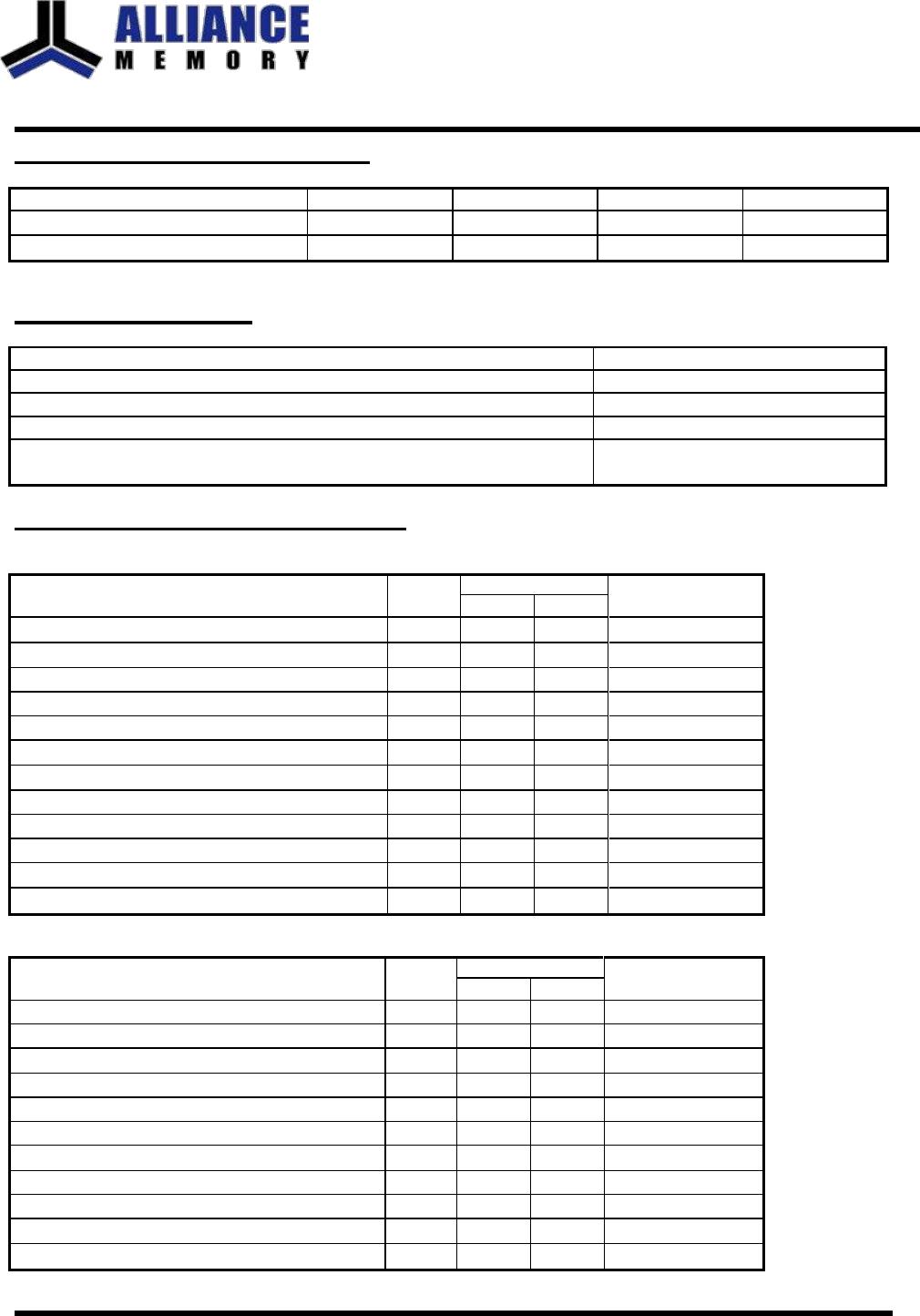
(1) READ CYCLE
PARAMETER
SYM.
AS7C316098A-10
UNIT
MIN.
MAX.
Read Cycle Time
tRC
10
-
ns
Address Access Time
tAA
-
10
ns
Chip Enable Access Time
t
ACE
-
10
ns
Output Enable Access Time
t
OE
-
4.5
ns
Chip Enable to Output in Low-Z
t
CLZ
*
2
-
ns
Output Enable to Output in Low-Z
tOLZ*
0
-
ns
Chip Disable to Output in High-Z
tCHZ*
-
4
ns
Output Disable to Output in High-Z
t
OHZ
*
-
4
ns
Output Hold from Address Change
t
OH
2
-
ns
LB#, UB# Access Time
t
BA
-
4.5
ns
LB#, UB# to High-Z Output
tBHZ*
-
4
ns
LB#, UB# to Low-Z Output
tBLZ*
0
-
ns
(2) WRITE CYCLE
*These parameters are guaranteed by device characterization, but not production tested.
Alliance Memory, Inc.
4
AS7C316098A
Rev. 1.2
1024K X 16 BIT HIGH SPEED CMOS SRAM
TIMING WAVEFORMS
READ CYCLE 1 (Address Controlled) (1,2)
t
RC
Address
t
AA
t
OH
Dout
Previous
Data
Valid
Data
Valid
READ CYCLE 2 (CE# and OE# Controlled) (1,3,4,5)
t
RC
Address
t
AA
CE#
t
ACE
LB#
,
UB#
t
BA
OE#
Dout
High-Z
t
BLZ
t
CLZ
t
OLZ
t
OE
t
OH
t
OHZ
t
BHZ
t
CHZ
Data Valid
High-Z
Notes :
1.WE#is high for read cycle.
2.Device is continuously selected OE# = low, CE# = low, LB# or UB# = low.
3.Address must be valid prior to or coincident with CE# = low, LB# or UB# = low transition; otherwise tAA is the limiting parameter.
4.tCLZ, tBLZ, tOLZ, tCHZ, tBHZ and tOHZ are specified with CL = 5pF. Transition is measured ±500mV from steady state.
5.At any given temperature and voltage condition, t
CHZ
is less than t
CLZ
, t
BHZ
is less than t
BLZ
, t
OHZ
is less
than
t
OLZ.
.
Alliance Memory, Inc.
5

AS7C316098A-10BINTR

Mfr. #:
Manufacturer:
Alliance Memory
Description:
SRAM 16M, 3.3V, 10ns FAST 1024K x 16 Asyn SRAM
Lifecycle:
New from this manufacturer.
Delivery:
DHL FedEx Ups TNT EMS
Payment:
T/T Paypal Visa MoneyGram Western Union