(Limits are 100% tested at T
A
= +25°C. Limits over the operating temperature range and relevant supply voltage range are guaranteed
by design and characterization. Specifications marked GBD are guaranteed by design and not production tested. Specifications to the
minimum and maximum operating temperature are guaranteed by design and are not production tested.)
Note 1: System requirement.
Note 2: Maximum allowable pullup resistance is a function of the number of 1-Wire devices in the system and 1-Wire recovery times.
The specified value here applies to systems with only one device and with the minimum 1-Wire recovery times.
Note 3: Value represents the internal parasite capacitance when V
PUP
is first applied. Once the parasite capacitance is charged, it does
not affect normal communication. Typically, during normal communication, the internal parasite capacitance is effectively ~100pF.
Note 4: Guaranteed by design and/or characterization only. Not production tested.
Note 5: V
TL
, V
TH
, and V
HY
are functions of the internal supply voltage, which is a function of V
PUP
, R
PUP
, 1-Wire timing, and capacitive
loading on IO. Lower V
PUP
, higher R
PUP
, shorter t
REC
, and heavier capacitive loading all lead to lower values of V
TL
, V
TH
, and V
HY
.
Note 6: Voltage below which, during a falling edge on IO, a logic-zero is detected.
Note 7: The voltage on IO must be less than or equal to V
ILMAX
at all times the master is driving IO to a logic-zero level.
Note 8: Voltage above which, during a rising edge on IO, a logic-one is detected.
Note 9: After V
TH
is crossed during a rising edge on IO, the voltage on IO must drop by at least V
HY
to be detected as logic-zero.
Note 10: The I-V characteristic is linear for voltages less than 1V.
Note 11: Applies to a single device attached to a 1-Wire line.
Note 12: t
REC
min covers operation at worst-case temperature V
PUP
, R
PUP
, C
X
, t
RSTL
, t
WOL
, and t
RL
. t
RECMIN
can be significantly
reduced under less extreme conditions. Contact the factory for more information.
Note 13: The earliest recognition of a negative edge is possible at t
REH
after V
TH
has been previously reached.
Note 14: Defines maximum possible bit rate. Equal to 1/(t
W0LMIN
+ t
RECMIN
).
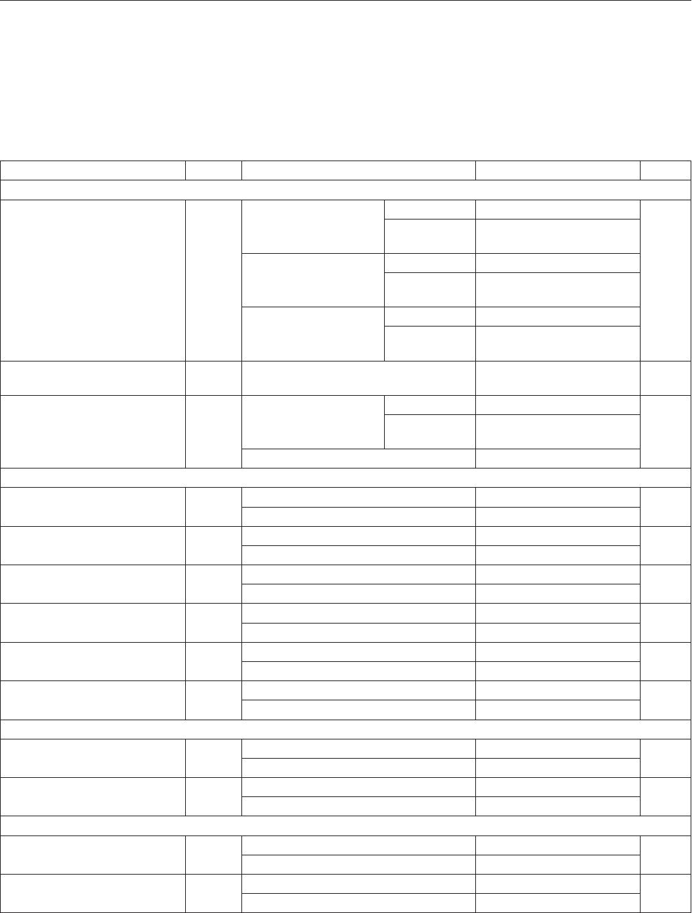
PARAMETER SYMBOL CONDITIONS MIN TYP MAX UNITS
GPIO PIN
GPIO Output Low PIOV
OL
PIOI
OL
= 4mA (Note 10) 0.4 V
GPIO Input Low PIOV
IL
-0.3 0.15 x V
PUP
V
GPIO Master Sample PIOV
IH
0.70 x V
PUP
V
PUP
+ 0.3 V
GPIO Switching Hysteresis PIOV
HY
0.3 V
GPIO Leakage Current PIOI
L
-10 +10 μA
STRONG PULLUP OPERATION
Strong Pullup Current I
SPU
(Note 19) 11 15 mA
Strong Pullup Voltage V
SPU
(Note 19) 2.8 V
Read Memory t
RM
2 ms
Write Memory t
WM
100 ms
Write State t
WS
15 ms
Computation Time (HMAC) t
CMP
4 ms
Generate ECC Key Pair t
GKP
350 ms
Generate ECDSA Signature t
GES
80 ms
Verify ECDSA Signature or
Compute ECDH Time
t
VES
160 ms
TRNG Generation t
RNG
40 ms
TRNG On-Demand Check t
ODC
65 ms
OTP
OTP Write Temperature T
OPTW
50 ºC
Data Retention t
DR
T
A
= +85°C (Note 21) 10 Years
POWER
Power-Up Time t
OSCWUP
(Notes 1, 20) 2 ms
Electrical Characteristics (continued)
www.maximintegrated.com
Maxim Integrated
│
5
DS28E83 DeepCover Radiation Resistant
1-Wire Authenticator