CY7C024E, CY7C0241E
CY7C025E, CY7C0251E
Document Number: 001-62932 Rev. *A Page 14 of 22
Notes
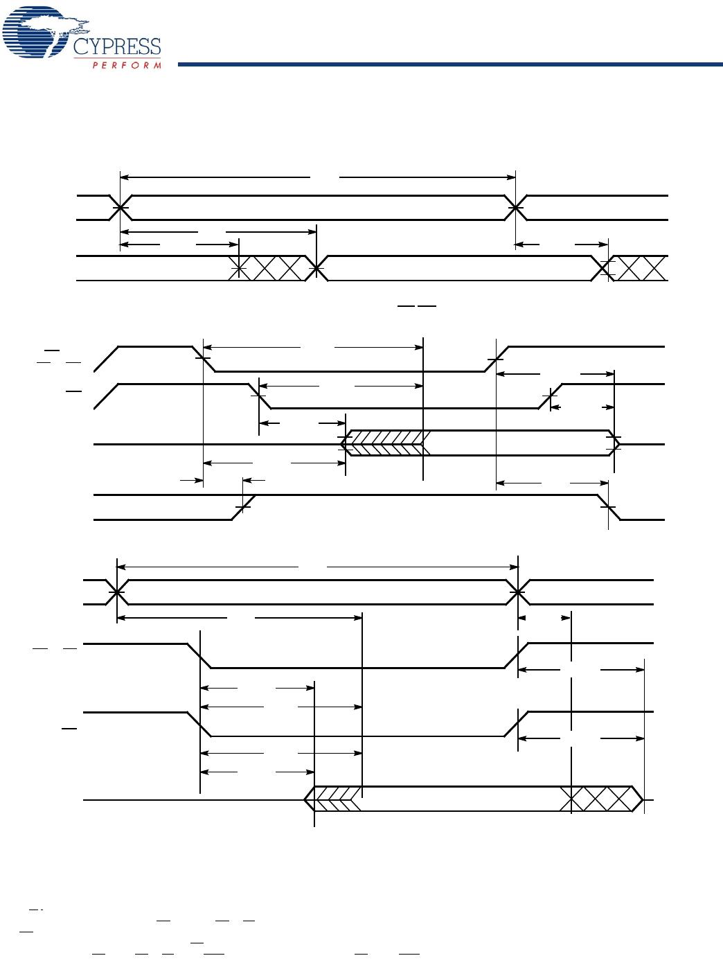
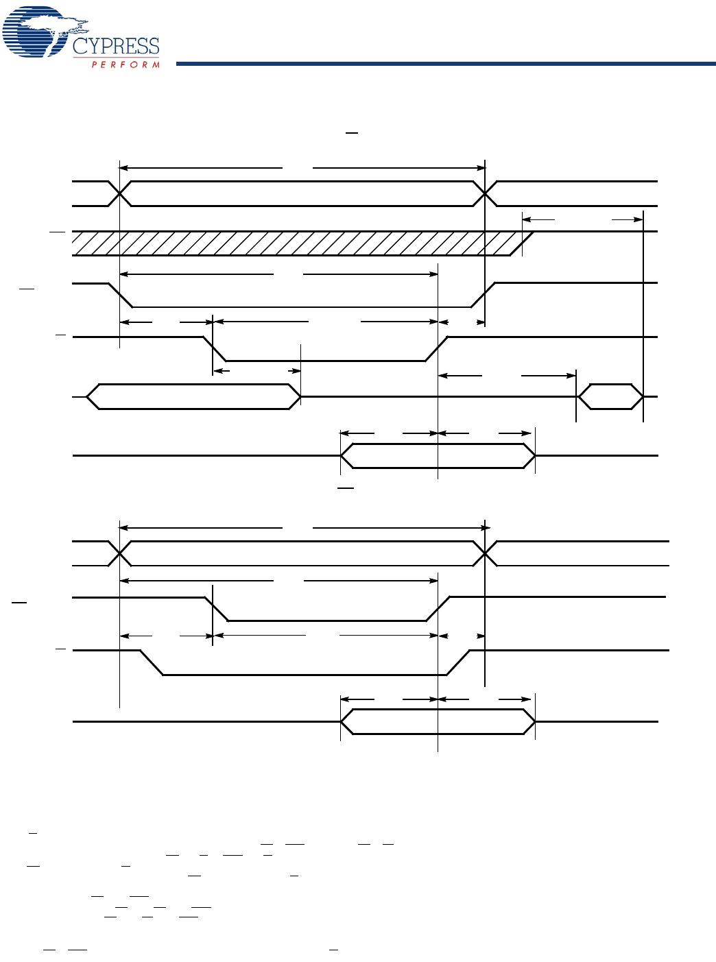
35. R/W
must be HIGH during all address transitions.
36. A write occurs during the overlap (t
SCE
or t
PWE
) of a LOW CE or SEM and a LOW UB or LB.
37. t
HA
is measured from the earlier of CE or R/W or (SEM or R/W) going HIGH at the end of write cycle.
38. If OE
is LOW during a R/W controlled write cycle, the write pulse width must be the larger of t
PWE
or (t
HZWE
+ t
SD
) to allow the I/O drivers to turn off and data to be
placed on the bus for the required t
SD
. If OE is HIGH during an R/W controlled write cycle, this requirement does not apply and the write pulse can be as short as
the specified t
PWE
.
39. To access RAM, CE
= V
IL
, SEM = V
IH
.
40. To access upper byte, CE
= V
IL
, UB = V
IL
, SEM = V
IH
.
To access lower byte, CE
= V
IL
, LB = V
IL
, SEM = V
IH
.
41. Transition is measured ±500 mV from steady state with a 5 pF load (including scope and jig). This parameter is sampled and not 100% tested.
42. During this period, the I/O pins are in the output state, and input signals must not be applied.
43. If the CE
or SEM LOW transition occurs simultaneously with or after the R/W LOW transition, the outputs remain in the high impedance state.
Switching Waveforms (continued)
t
AW
t
WC
t
PWE
t
HD
t
SD
t
HA
CE
R/W
OE
DATAOUT
DATA IN
ADDRESS
t
HZOE
t
SA
t
HZWE
t
LZWE
Figure 7. Write Cycle No. 1: R/W Controlled Timing
[35,36, 37, 38]
[41]
[41]
[38]
[39,40]
NOTE 42
NOTE 42
t
AW
t
WC
t
SCE
t
HD
t
SD
t
HA
CE
R/W
DATA IN
ADDRESS
t
SA
Figure 8. Write Cycle No. 2: CE Controlled Timing
[35, 36, 37,43]
[39,40]