CY7C024E, CY7C0241E
CY7C025E, CY7C0251E
Document Number: 001-62932 Rev. *A Page 7 of 22
When writing to the semaphore, only I/O
0
is used. If a zero is
written to the left port of an available semaphore, a one appears
at the same semaphore address on the right port. That
semaphore can now only be modified by the side showing zero
(the left port in this case). If the left port now relinquishes control
by writing a one to the semaphore, the semaphore is set to one
for both sides. However, if the right port had requested the
semaphore (written a zero) while the left port had control, the
right port immediately owns the semaphore as soon as the left
port releases it. Table 3 on page 8 shows sample semaphore
operations.
When reading a semaphore, all 16/18 data lines output the
semaphore value. The read value is latched in an output register
to prevent the semaphore from changing state during a write
from the other port. If both ports attempt to access the
semaphore within t
SPS
of each other, the semaphore is definitely
obtained by one side or the other, but there is no guarantee which
side controls the semaphore.
Notes
9. I/O
0
–I/O
8
on the CY7C0241E/CY7C0251E.
10. I/O
9
–I/O
17
on the CY7C0241E/CY7C0251E.
Table 1. Non-Contending Read/Write
Inputs Outputs
Operation
CE R/W OE UB LB SEM I/O
0
I/O
7
[9]
I/O
8
I/O
15
[10]
H X X X X H High Z High Z Deselected: power-down
X X X H H H High Z High Z Deselected: power-down
L L X L H H High Z Data in Write to upper byte only
L L X H L H Data in High Z Write to lower byte only
L L X L L H Data in Data in Write to both bytes
L H L L H H High Z Data out Read upper byte only
L H L H L H Data out High Z Read lower byte only
L H L L L H Data out Data out Read both bytes
X X H X X X High Z High Z Outputs disabled
H H L X X L Data out Data out Read data in semaphore flag
X H L H H L Data out Data out Read data in semaphore flag
H X X X L Data in Data in Write D
IN0
into semaphore flag
X X H H L Data in Data in Write D
IN0
into semaphore flag
L X X L X L Not allowed
L X X X L L Not allowed
CY7C024E, CY7C0241E
CY7C025E, CY7C0251E
Document Number: 001-62932 Rev. *A Page 8 of 22
Table 2. Interrupt Operation Example (Assumes BUSY
L
=BUSY
R
=HIGH)
[11]
Function
Left Port Right Port
R/W
L
CE
L
OE
L
A
0L–11L
INT
L
R/W
R
CE
R
OE
R
A
0R–11R
INT
R
Set right INT
R
flag L L X (1)FFF X X X X X L
[12]
Reset right INT
R
flag XXXXXXLL(1)FFFH
[13]
Set left INT
L
flag X X X X L
[13]
LLX(1)FFEX
Reset left INT
L
flag X L L (1)FFE H
[12]
XXX X X
Table 3. Semaphore Operation Example
Function
I/O
0
I/O
15/17
Left
I/O
0
I/O
15/17
Right
Status
No action 1 1 Semaphore-free
Left port writes 0 to semaphore 0 1 Left port has semaphore token
Right port writes 0 to semaphore 0 1 No change. Right side has no write access to semaphore.
Left port writes 1 to semaphore 1 0 Right port obtains semaphore token
Left port writes 0 to semaphore 1 0 No change. Left port has no write access to semaphore
Right port writes 1 to semaphore 0 1 Left port obtains semaphore token
Left port writes 1 to semaphore 1 1 Semaphore-free
Right port writes 0 to semaphore 1 0 Right port has semaphore token
Right port writes 1 to semaphore 1 1 Semaphore-free
Left port writes 0 to semaphore 0 1 Left port has semaphore token
Left port writes 1 to semaphore 1 1 Semaphore-free
Notes
11. A
0L–12L
and A
0R–12R
, 1FFF/1FFE for the CY7C025E/CY7C0251E.
12. If BUSY
L
=L, then no change.
13. BUSY
R
=L, then no change.If
CY7C024E, CY7C0241E
CY7C025E, CY7C0251E
Document Number: 001-62932 Rev. *A Page 9 of 22
Maximum Ratings
Exceeding maximum ratings may shorten the useful life of the
device. User guidelines are not tested.
[14]
Storage temperature ................................ –65 °C to +150 °C
Ambient temperature with
power applied........................................... –55 °C to +125 °C
Supply voltage to ground potential ...............–0.3 V to +7.0 V
DC voltage applied to outputs
in high Z state...............................................–0.5 V to +7.0 V
DC input voltage
[15]
......................................–0.5 V to +7.0 V
Output current into outputs (LOW) .............................. 20 mA
Static discharge voltage.......................................... > 2001 V
(per MIL-STD-883, Method 3015)
Latch-up current .................................................... > 200 mA
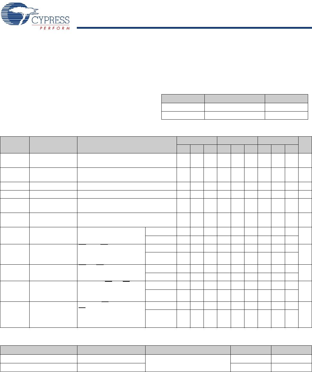
Operating Range
Range Ambient Temperature V
CC
Commercial 0 °C to +70 °C 5 V 10%
Industrial –40 °C to +85 °C 5 V 10%
Notes
14. The voltage on any input or I/O pin cannot exceed the power pin during power-up.
15. Pulse width < 20 ns.
16. f
MAX
= 1/t
RC
= All inputs cycling at f = 1/t
RC
(except output enable). f = 0 means no address or control lines change. This applies only to inputs at CMOS level
standby I
SB3.
17. Tested initially and after any design or process changes that may affect these parameters.
Electrical Characteristics Over the Operating Range
Parameter Description Test Conditions
–15 –25 –55
Unit
Min Typ Max Min Typ Max Min Typ Max
V
OH
Output HIGH
voltage
V
CC
= Min, I
OH
= –4.0 mA 2.4 2.4 2.4 V
V
OL
Output LOW
voltage
V
CC
= Min, I
OL
= 4.0 mA 0.4 0.4 0.4 V
V
IH
Input HIGH voltage 2.2 2.2 2.2 V
V
IL
Input LOW voltage –0.7 0.8 –0.7 0.8 –0.7 0.8 V
I
IX
Input leakage
current
GND V
I
V
CC
–10 +10 –10 +10 –10 +10 A
I
OZ
Output leakage
current
Output disabled,
GND V
O
V
CC
–10 +10 –10 +10 –10 +10 A
I
CC
Operating current V
CC
= Max, I
OUT
= 0 mA,
Outputs Disabled
Commercial 190 285 170 250 150 230 mA
Industrial 215 305 180 290 180 290
I
SB1
Standby current
(both ports TTL
levels)
CE
L
and CE
R
V
IH
,
f = f
MAX
[16]
Commercial 50 70 40 60 20 50 mA
Industrial 65 95 55 80 55 80
I
SB2
Standby current
(one port TTL level)
CE
L
or CE
R
V
IH
,
f = f
MAX
[16]
Commercial 120 180 100 150 75 135 mA
Industrial 135 205 120 175 120 175
I
SB3
Standby current
(both ports CMOS
levels)
Both Ports CE
and CE
R
V
CC
– 0.2 V, V
IN
V
CC
– 0.2 V
or V
IN
0.2 V, f = 0
[16]
Commercial 0.05 0.5 0.05 0.50 0.05 0.50 mA
Industrial 0.05 0.5 0.05 0.50 0.05 0.50
I
SB4
Standby current
(both ports CMOS
levels)
One Port CE
L
or
CE
R
V
CC
– 0.2 V,
V
IN
 V
CC
– 0.2 V or V
IN
0.2 V,
Active Port Outputs, f = f
MAX
[16]
Commercial 110 160 90 130 70 120 mA
Industrial 125 175 110 150 110 150
Capacitance
Parameter
[17]
Description Test Conditions Max Unit
C
IN
Input capacitance T
A
= 25 °C , f = 1 MHz,
V
CC
= 5.0 V
10 pF
C
OUT
Output capacitance 10 pF

CY7C0241E-15AXCT

Mfr. #:
Manufacturer:
Cypress Semiconductor
Description:
IC SRAM 72K PARALLEL 100TQFP
Lifecycle:
New from this manufacturer.
Delivery:
DHL FedEx Ups TNT EMS
Payment:
T/T Paypal Visa MoneyGram Western Union